JAJSV18 July 2024 TCAN1473A-Q1
ADVANCE INFORMATION
- 1
- 1 特長
- 2 アプリケーション
- 3 概要
- 4 Pin Configuration and Functions
-
5 Specifications
- 5.1 Absolute Maximum Ratings
- 5.2 ESD Ratings
- 5.3 ESD Ratings - IEC Specifications
- 5.4 Recommended Operating Conditions
- 5.5 Thermal Information
- 5.6 Power Dissipation Ratings
- 5.7 Power Supply Characteristics
- 5.8 Electrical Characteristics
- 5.9 Timing Requirements
- 5.10 Switching Characteristics
- 5.11 Typical Characteristics
- 6 Parameter Measurement Information
-
7 Detailed Description
- 7.1 Overview
- 7.2 Functional Block Diagram
- 7.3
Feature Description
- 7.3.1 Supply Pins
- 7.3.2 Digital Inputs and Outputs
- 7.3.3 GND
- 7.3.4 INH Pin
- 7.3.5 WAKE Pin
- 7.3.6 CAN Bus Pins
- 7.3.7
Faults
- 7.3.7.1
Internal and External Fault Indicators
- 7.3.7.1.1 Power-Up (PWRON Flag)
- 7.3.7.1.2 Wake-Up Request (WAKERQ Flag)
- 7.3.7.1.3 Undervoltage Faults
- 7.3.7.1.4 CAN Bus Fault (CBF Flag)
- 7.3.7.1.5 TXD Clamped Low (TXDCLP Flag)
- 7.3.7.1.6 TXD Dominant State Timeout (TXDDTO Flag)
- 7.3.7.1.7 TXD Shorted to RXD Fault (TXDRXD Flag)
- 7.3.7.1.8 CAN Bus Dominant Fault (CANDOM Flag)
- 7.3.7.1
Internal and External Fault Indicators
- 7.3.8 Local Faults
- 7.4 Device Functional Modes
- 8 Application Information Disclaimer
- 9 Device and Documentation Support
- 10Revision History
- 11Mechanical, Packaging, and Orderable Information
パッケージ・オプション
デバイスごとのパッケージ図は、PDF版データシートをご参照ください。
メカニカル・データ(パッケージ|ピン)
- D|14
- DYY|14
- DMT|14
サーマルパッド・メカニカル・データ
発注情報
7.4.1.5.1 Remote Wake Request via Wake-Up Pattern (WUP)
The TCAN1473A-Q1 implements a low-power wake receiver in the standby and sleep mode that uses the multiple filtered dominant wake-up pattern (WUP) defined in the ISO11898-2:2016 standard.
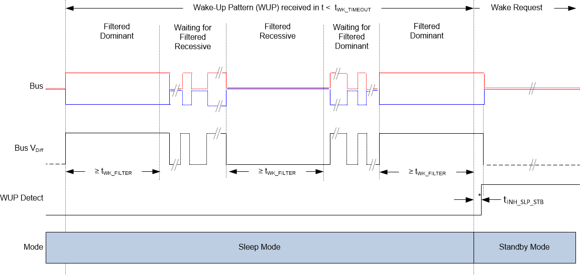
The wake-up pattern (WUP) consists of a filtered dominant bus, then a filtered recessive bus time followed by a second filtered dominant bus time. The first filtered dominant initiates the WUP and the bus monitor is now waiting on a filtered recessive; other bus traffic will not reset the bus monitor. Once a filtered recessive is received the bus monitor is now waiting on a filtered dominant, and again, other bus traffic will not reset the bus monitor. Immediately upon receiving of the second filtered dominant the bus monitor will recognize the WUP and drive the RXD terminal low, if a valid VIO is present signaling to the controller the wake-up request. If a valid VIO is not present when the wake-up pattern is received the transceiver drives the RXD output pin low once VIO > UVIOR.
The WUP consists of:
- A filtered dominant bus of at least tWK(FILTER) followed by
- A filtered recessive bus time of at least tWK(FILTER) followed by
- A second filtered dominant bus time of at least tWK(FILTER)
For a dominant or recessive to be considered “filtered,” the bus must be in that state for more than tWK(FILTER) time. Due to variability in the tWK(FILTER) the following scenarios are applicable. Bus state times less than the tWK(FILTER) minimum will never be detected as part of a WUP and thus no wake request will be generated. Bus state times between tWK(FILTER) minimum and tWK(FILTER) maximum may be detected as part of a WUP and a wake request may be generated. Bus state times more than tWK(FILTER) maximum will always be detected as part of a WUP and thus a wake request will always be generated. See Figure 7-6 for the timing diagram of the WUP.
The pattern and tWK(FILTER) time used for the WUP and wake request prevents noise and bus stuck dominant faults from causing false wake requests while allowing any CAN or CAN FD message to initiate a wake request.
ISO11898-2:2016 has two sets of times for a short and long wake-up filter times. The tWK(FILTER) timing for the TCAN1473A-Q1 has been picked to be within the min and max values of both filter ranges. This timing has been chosen such that a single bit time at 500kbps, or two back to back bit times at 1Mbps triggers the filter in either bus state.
For an additional layer of robustness and to prevent false wake-ups, the transceiver implements the tWK(TIMEOUT) timer. For a remote wake-up event to successfully occur, the entire wake-up pattern must be received within the timeout value. If the full wake-up pattern is not received before the tWK(TIMEOUT) expires then the internal logic is reset and the transceiver remains in sleep mode without waking up. The full pattern must then be transmitted again within the tWK(TIMEOUT) window. See Figure 7-6.
A recessive bus of at least tWK(FILTER) must separate the next WUP pattern if the CAN bus is dominant when the tWK(TIMEOUT) expires.
