JAJSGQ7A
December 2018 – January 2020
TCAN4550
PRODUCTION DATA.
1
特長
2
アプリケーション
3
概要
Device Images
概略回路図、MUC から CLKIN
概略回路図、水晶振動子
4
改訂履歴
5
概要(続き)
6
Pin Configuration and Functions
Pin Functions
7
Specifications
7.1
Absolute Maximum Ratings
7.2
ESD Ratings
7.3
ESD Ratings, IEC ESD and ISO Transient Specification
7.4
Recommended Operating Conditions
7.5
Thermal Information
7.6
Supply Characteristics
7.7
Electrical Characteristics
7.8
Timing Requirements
7.9
Switching Characteristics
7.10
Typical Characteristics
8
Parameter Measurement Information
9
Detailed Description
9.1
Overview
9.2
Functional Block Diagram
9.3
Feature Description
9.3.1
VSUP Pin
9.3.2
VIO Pin
9.3.3
VCCOUT Pin
9.3.4
GND
9.3.5
INH Pin
9.3.6
WAKE Pin
9.3.7
FLTR Pin
9.3.8
RST Pin
9.3.9
OSC1 and OSC2 Pins
9.3.10
nWKRQ Pin
9.3.11
nINT Interrupt Pin
9.3.12
GPO1 Pin
9.3.13
GPO2 Pin
9.3.14
CANH and CANL Bus Pins
9.4
Device Functional Modes
9.4.1
Normal Mode
9.4.2
Standby Mode
9.4.3
Sleep Mode
9.4.3.1
Bus Wake via RXD_INT Request (BWRR) in Sleep Mode
9.4.3.2
Local Wake Up (LWU) via WAKE Input Terminal
9.4.4
Test Mode
9.4.5
Failsafe Feature
9.4.6
Protection Features
9.4.6.1
Watchdog Function
9.4.6.2
Driver and Receiver Function
9.4.6.3
Floating Terminals
9.4.6.4
TXD_INT Dominant Timeout (DTO)
9.4.6.5
CAN Bus Short Circuit Current Limiting
9.4.6.6
Thermal Shutdown
9.4.6.7
Under Voltage Lockout (UVLO) and Unpowered Device
9.4.6.7.1
UVSUP and UVCCOUT
9.4.6.7.2
UVIO
9.4.6.7.3
Fault and M_CAN Core Behavior:
9.4.7
CAN FD
9.5
Programming
9.5.1
SPI Communication
9.5.1.1
Chip Select Not (nCS):
9.5.1.2
SPI Clock Input (SCLK):
9.5.1.3
SPI Data Input (SDI):
9.5.1.4
SPI Data Output (SDO):
9.5.2
Register Descriptions
9.6
Register Maps
9.6.1
Device ID and Interrupt/Diagnostic Flag Registers: 16'h0000 to 16'h002F
9.6.1.1
DEVICE_ID1[31:0] (address = h0000) [reset = h4E414354]
Table 10.
Device ID Field Descriptions
9.6.1.2
DEVICE_ID2[31:0] (address = h0004) [reset = h30353534]
Table 11.
Device ID Field Descriptions
9.6.1.3
Revision (address = h0008) [reset = h00110201]
Table 12.
Revision Field Descriptions
9.6.1.4
Status (address = h000C) [reset = h0000000U]
Table 13.
Status Field Descriptions
9.6.2
Device Configuration Registers: 16'h0800 to 16'h08FF
9.6.2.1
Modes of Operation and Pin Configuration Registers (address = h0800) [reset = hC8000468]
Table 15.
Modes of Operation and Pin Configuration Registers Field Descriptions
9.6.2.2
Timestamp Prescalar (address = h0804) [reset = h00000002]
Table 16.
EMC Enhancement and Timestamp Prescalar Field Descriptions
9.6.2.3
Test Register and Scratch Pad (address = h0808) [reset = h00000000]
Table 17.
Test and Scratch Pad Register Field Descriptions
9.6.2.4
Test Register (address = h080C) [reset = h00000000]
Table 18.
Test Register Field Descriptions
9.6.3
Interrupt/Diagnostic Flag and Enable Flag Registers: 16'h0820/0824 and 16'h0830
9.6.3.1
Interrupts (address = h0820) [reset = h00100000]
Table 19.
Interrupts Field Descriptions
9.6.3.2
MCAN Interrupts (address = h0824) [reset = h00000000]
Table 20.
MCAN Interrupts Field Descriptions
9.6.3.3
Interrupt Enables (address = h0830 ) [reset = hFFFFFFFF]
Table 21.
Interrupt Enables Field Descriptions
9.6.4
CAN FD Register Set: 16'h1000 to 16'h10FF
9.6.4.1
Core Release Register (address = h1000) [reset = hrrrddddd]
Table 25.
Core Release Register Field Descriptions
9.6.4.2
Endian Register (address = h1004) [reset = h87654321]
Table 26.
Endian Register Field Descriptions
9.6.4.3
Customer Register (address = h1008) [reset = h00000000]
Table 27.
Customer Register Field Descriptions
9.6.4.4
Data Bit Timing & Prescaler (address = h100C) [reset = h0000A33]
Table 28.
Data Bit Timing & Prescaler Field Descriptions
9.6.4.5
Test Register (address = h1010 ) [reset = h00000000]
Table 29.
Test Register Field Descriptions
9.6.4.6
RAM Watchdog (address = h1014) [reset = h00000000]
Table 30.
RAM Watchdog Field Descriptions
9.6.4.7
Control Register (address = h1018) [reset = 0000 0019]
Table 31.
Control Register Field Descriptions
9.6.4.8
Nominal Bit Timing & Prescaler Register (address = h101C) [reset = h06000A03]
Table 32.
Nominal Bit Timing & Prescaler Register Field Descriptions
9.6.4.9
Timestamp Counter Configuration (address = h1020) [reset = h00000000]
Table 33.
Timestamp Counter Configuration Descriptions
9.6.4.10
Timestamp Counter Value (address = h1024) [reset = h00000000]
Table 34.
Timestamp Counter Value Field Descriptions
9.6.4.11
Timeout Counter Configuration (address = h1028) [reset = hFFFF0000]
Table 35.
Timeout Counter Configuration Field Descriptions
9.6.4.12
Timeout Counter Value (address = h102C) [reset = h0000FFFF]
Table 36.
Timeout Counter Value Field Descriptions
9.6.4.13
Reserved (address = h1030 - h103C) [reset = h00000000]
Table 37.
Reserved Field Descriptions
9.6.4.14
Error Counter Register (address = h1040) [reset = h00000000]
Table 38.
Error Counter Register Field Descriptions
9.6.4.15
Protocol Status Register (address = h1044) [reset = h00000707]
Table 39.
Protocol Status Register Field Descriptions
9.6.4.16
Transmitter Delay Compensation Register (address = h1048) [reset = h00000000]
Table 40.
Transmitter Delay Compensation Register Field Descriptions
9.6.4.17
Reserved (address = h104C) [reset = h00000000]
Table 41.
Reserved Field Descriptions
9.6.4.18
Interrupt Register (address = h1050) [reset = h00000000]
Table 42.
Interrupt Register Field Descriptions
9.6.4.19
Interrupt Enable (address = h1054) [reset = h00000000]
Table 43.
Interrupt Enable Field Descriptions
9.6.4.20
Interrupt Line Select (address = h1058) [reset = h00000000]
Table 44.
Interrupt Line Select Field Descriptions
9.6.4.21
Interrupt Line Enable (address = h105C) [reset = h00000000]
Table 45.
Interrupt Line Enable Field Descriptions
9.6.4.22
Reserved (address = h1060 - h107C) [reset = h00000000]
Table 46.
Reserved Field Descriptions
9.6.4.23
Global Filter Configuration (address = h1080) [reset = h00000000]
Table 47.
Global Filter Configuration Field Descriptions
9.6.4.24
Standard ID Filter Configuration (address = h1084) [reset = h00000000]
Table 48.
Standard ID Filter Configuration Field Descriptions
9.6.4.25
Extended ID Filter Configuration (address = h1088) [reset = h00000000]
Table 49.
Extended ID Filter Configuration Field Descriptions
9.6.4.26
Reserved (address = h108C) [reset = h00000000]
Table 50.
Reserved Field Descriptions
9.6.4.27
Extended ID AND Mask (address = h1090) [reset = h1FFFFFFF]
Table 51.
Extended ID AND Mask Field Descriptions
9.6.4.28
High Priority Message Status (address = h1094) [reset = h00000000]
Table 52.
High Priority Message Status Field Descriptions
9.6.4.29
New Data 1 (address = h1098) [reset = h00000000]
Table 53.
New Data 1 Field Descriptions
9.6.4.30
New Data 2 (address = h109C) [reset = h00000000]
Table 54.
New Data 2 Field Descriptions
9.6.4.31
Rx FIFO 0 Configuration (address = h10A0) [reset = h00000000]
Table 55.
Rx FIFO 0 Configuration Field Descriptions
9.6.4.32
Rx FIFO 0 Status (address = h10A4) [reset = h00000000]
Table 56.
Rx FIFO 0 Status Field Descriptions
9.6.4.33
Rx FIFO 0 Acknowledge (address = h10A8) [reset = h00000000]
Table 57.
Rx FIFO 0 Acknowledge Field Descriptions
9.6.4.34
Rx Buffer Configuration (address = h10AC) [reset = h00000000]
Table 58.
Rx Buffer Configuration Field Descriptions
9.6.4.35
Rx FIFO 1 Configuration (address = h10B0) [reset = h00000000]
Table 59.
Rx FIFO 1 Configuration Field Descriptions
9.6.4.36
Rx FIFO 1 Status (address = h10B4) [reset = h00000000]
Table 60.
Rx FIFO 1 Status Field Descriptions
9.6.4.37
Rx FIFO 1 Acknowledge (address = h10B8) [reset = h00000000]
Table 61.
Rx FIFO 1 Acknowledge Field Descriptions
9.6.4.38
Rx Buffer/FIFO Element Size Configuration (address = h10BC) [reset = h00000000]
Table 62.
Rx Buffer/FIFO Element Size Configuration Field Descriptions
9.6.4.39
Tx Buffer Configuration (address = h10C0) [reset = h00000000]
Table 63.
Tx Buffer Configuration Field Descriptions
9.6.4.40
Tx FIFO/Queue Status (address = h10C4) [reset = h00000000]
Table 64.
Tx FIFO/Queue Status Field Descriptions
9.6.4.41
Tx Buffer Element Size Configuration (address = h10C8) [reset = h00000000]
Table 65.
Tx Buffer Element Size Configuration Field Descriptions
9.6.4.42
Tx Buffer Request Pending (address = h10CC) [reset = h00000000]
Table 66.
Tx Buffer Request Pending Field Descriptions
9.6.4.43
Tx Buffer Add Request (address = h10D0) [reset = h00000000]
Table 67.
Tx Buffer Add Request Field Descriptions
9.6.4.43.1
Tx Buffer Cancellation Request (address = h10D4 [reset = h00000000]
Table 68.
Tx Buffer Cancellation Request Field Descriptions
9.6.4.43.2
Tx Buffer Add Request Transmission Occurred (address = h10D8) [reset = h00000000]
Table 69.
Tx Buffer Add Request Transmission Occurred Field Descriptions
9.6.4.43.3
Tx Buffer Cancellation Finished (address = h10DC) [reset = h00000000]
Table 70.
Tx Buffer Cancellation Finished Field Descriptions
9.6.4.43.4
Tx Buffer Transmission Interrupt Enable (address = h10E0) [reset = h00000000]
Table 71.
Tx Buffer Transmission Interrupt Enable Field Descriptions
9.6.4.43.5
Tx Buffer Cancellation Finished Interrupt Enable (address = h10E4) [reset = h00000000]
Table 72.
Tx Buffer Cancellation Finished Interrupt Enable Field Descriptions
9.6.4.43.6
Reserved (address = h10E8) [reset = h00000000]
Table 73.
Reserved Field Descriptions
9.6.4.43.7
Reserved (address = h10EC) [reset = h00000000]
Table 74.
Reserved Field Descriptions
9.6.4.43.8
Tx Event FIFO Configuration (address = h10F0) [reset = h00000000]
Table 75.
Tx Event FIFO Configuration Field Descriptions
9.6.4.43.9
Tx Event FIFO Status (address = h10F4) [reset = h00000000]
Table 76.
Tx Event FIFO Status Field Descriptions
9.6.4.43.10
Tx Event FIFO Acknowledge (address = h10F8) [reset = h00000000]
Table 77.
Tx Event FIFO Acknowledge Field Descriptions
9.6.4.43.11
Reserved (address = h10FC) [reset = h00000000]
Table 78.
Reserved Field Descriptions
10
Application and Implementation
10.1
Application Design Consideration
10.1.1
Crystal and Clock Input Requirements
10.1.2
Bus Loading, Length and Number of Nodes
10.1.3
CAN Termination
10.1.3.1
Termination
10.1.3.2
CAN Bus Biasing
10.1.4
INH Brownout Behavior
10.2
Typical Application
10.2.1
Detailed Requirements
10.2.2
Detailed Design Procedures
10.2.3
Application Curves
10.2.4
Application Curves
11
Power Supply Recommendations
12
Layout
12.1
Layout Guidelines
12.2
Layout Example
13
デバイスおよびドキュメントのサポート
13.1
ドキュメントのサポート
13.1.1
関連資料
13.1.1.1
CAN トランシーバの物理層の標準
13.1.1.2
EMC要件
13.1.1.3
準拠テストの要件
13.1.1.4
サポート・ドキュメント
13.2
ドキュメントの更新通知を受け取る方法
13.3
サポート・リソース
13.4
商標
13.5
静電気放電に関する注意事項
13.6
Glossary
14
メカニカル、パッケージ、および注文情報
パッケージ・オプション
メカニカル・データ(パッケージ|ピン)
RGY|20
MPQF116H
サーマルパッド・メカニカル・データ
RGY|20
QFND599
発注情報
jajsgq7a_oa
jajsgq7a_pm
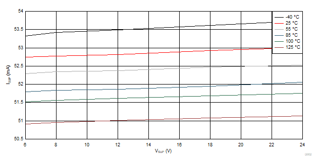
10.2.3
Application Curves
V
CCOUT
= Off
CAN Bus State = Dominant
CAN Bus Load = 60 Ω
Figure 109.
I
SUP
Across V
SUP
and Temperature
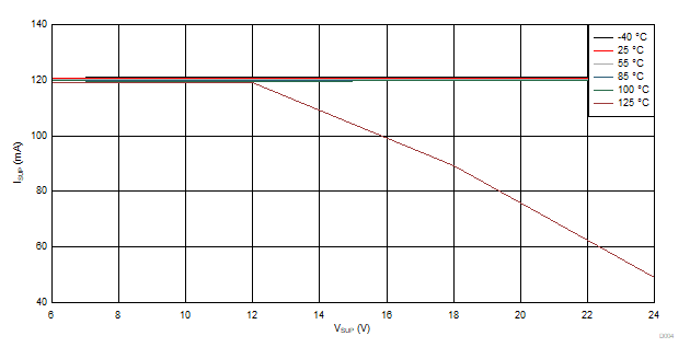
I
CCOUT
= 70 mA
CAN Bus State = Dominant
CAN Bus Load = 60 Ω
Figure 110.
I
SUP
Across V
SUP
, Temperature and V
CCOUT
with Maximum Load Current