JAJSGK9F December 2015 – May 2019 TDA2HF , TDA2HG , TDA2HV , TDA2LF , TDA2SA , TDA2SG , TDA2SX
PRODUCTION DATA.
- 1 デバイスの概要
- 2 改訂履歴
- 3 Device Comparison
-
4 Terminal Configuration and Functions
- 4.1 Terminal Assignment
- 4.2 Ball Characteristics
- 4.3 Multiplexing Characteristics
- 4.4
Signal Descriptions
- 4.4.1 Video Input Port (VIP)
- 4.4.2 Display Subsystem – Video Output Ports
- 4.4.3 Display Subsystem – High-Definition Multimedia Interface (HDMI)
- 4.4.4 External Memory Interface (EMIF)
- 4.4.5 General-Purpose Memory Controller (GPMC)
- 4.4.6 Timers
- 4.4.7 Inter-Integrated Circuit Interface (I2C)
- 4.4.8 Universal Asynchronous Receiver Transmitter (UART)
- 4.4.9 Multichannel Serial Peripheral Interface (McSPI)
- 4.4.10 Quad Serial Peripheral Interface (QSPI)
- 4.4.11 Multichannel Audio Serial Port (McASP)
- 4.4.12 Universal Serial Bus (USB)
- 4.4.13 SATA
- 4.4.14 Peripheral Component Interconnect Express (PCIe)
- 4.4.15 Controller Area Network Interface (DCAN)
- 4.4.16 Ethernet Interface (GMAC_SW)
- 4.4.17 eMMC/SD/SDIO
- 4.4.18 General-Purpose Interface (GPIO)
- 4.4.19 Pulse Width Modulation (PWM) Interface
- 4.4.20 System and Miscellaneous
- 4.4.21 Test Interfaces
-
5 Specifications
- 5.1 Absolute Maximum Ratings
- 5.2 ESD Ratings
- 5.3 Power on Hour (POH) Limits
- 5.4 Recommended Operating Conditions
- 5.5 Operating Performance Points
- 5.6 Power Consumption Summary
- 5.7
Electrical Characteristics
- 5.7.1 LVCMOS DDR DC Electrical Characteristics
- 5.7.2 HDMIPHY DC Electrical Characteristics
- 5.7.3 Dual Voltage LVCMOS I2C DC Electrical Characteristics
- 5.7.4 IQ1833 Buffers DC Electrical Characteristics
- 5.7.5 IHHV1833 Buffers DC Electrical Characteristics
- 5.7.6 LVCMOS OSC Buffers DC Electrical Characteristics
- 5.7.7 BC1833IHHV Buffers DC Electrical Characteristics
- 5.7.8 USBPHY DC Electrical Characteristics
- 5.7.9 Dual Voltage SDIO1833 DC Electrical Characteristics
- 5.7.10 Dual Voltage LVCMOS DC Electrical Characteristics
- 5.7.11 SATAPHY DC Electrical Characteristics
- 5.7.12 PCIEPHY DC Electrical Characteristics
- 5.8 Thermal Resistance Characteristics
- 5.9 Power Supply Sequences
- 6 Clock Specifications
-
7 Timing Requirements and Switching Characteristics
- 7.1 Timing Test Conditions
- 7.2 Interface Clock Specifications
- 7.3 Timing Parameters and Information
- 7.4 Recommended Clock and Control Signal Transition Behavior
- 7.5 Virtual and Manual I/O Timing Modes
- 7.6 Video Input Ports (VIP)
- 7.7 Display Subsystem – Video Output Ports
- 7.8 Display Subsystem – High-Definition Multimedia Interface (HDMI)
- 7.9 External Memory Interface (EMIF)
- 7.10 General-Purpose Memory Controller (GPMC)
- 7.11 Timers
- 7.12 Inter-Integrated Circuit Interface (I2C)
- 7.13 Universal Asynchronous Receiver Transmitter (UART)
- 7.14 Multichannel Serial Peripheral Interface (McSPI)
- 7.15 Quad Serial Peripheral Interface (QSPI)
- 7.16
Multichannel Audio Serial Port (McASP)
- Table 7-45 Timing Requirements for McASP1
- Table 7-46 Timing Requirements for McASP2
- Table 7-47 Timing Requirements for McASP3/4/5/6/7/8
- Table 7-48 Switching Characteristics Over Recommended Operating Conditions for McASP1
- Table 7-49 Switching Characteristics Over Recommended Operating Conditions for McASP2
- Table 7-50 Switching Characteristics Over Recommended Operating Conditions for McASP3/4/5/6/7/8
- 7.17 Universal Serial Bus (USB)
- 7.18 Serial Advanced Technology Attachment (SATA)
- 7.19 Peripheral Component Interconnect Express (PCIe)
- 7.20 Controller Area Network Interface (DCAN)
- 7.21
Ethernet Interface (GMAC_SW)
- 7.21.1
GMAC MII Timings
- Table 7-67 Timing Requirements for miin_rxclk - MII Operation
- Table 7-68 Timing Requirements for miin_txclk - MII Operation
- Table 7-69 Timing Requirements for GMAC MIIn Receive 10/100 Mbit/s
- Table 7-70 Switching Characteristics Over Recommended Operating Conditions for GMAC MIIn Transmit 10/100 Mbits/s
- 7.21.2 GMAC MDIO Interface Timings
- 7.21.3
GMAC RMII Timings
- Table 7-75 Timing Requirements for GMAC REF_CLK - RMII Operation
- Table 7-76 Timing Requirements for GMAC RMIIn Receive
- Table 7-77 Switching Characteristics Over Recommended Operating Conditions for GMAC REF_CLK - RMII Operation
- Table 7-78 Switching Characteristics Over Recommended Operating Conditions for GMAC RMIIn Transmit 10/100 Mbits/s
- 7.21.4
GMAC RGMII Timings
- Table 7-82 Timing Requirements for rgmiin_rxc - RGMIIn Operation
- Table 7-83 Timing Requirements for GMAC RGMIIn Input Receive for 10/100/1000 Mbps
- Table 7-84 Switching Characteristics Over Recommended Operating Conditions for rgmiin_txctl - RGMIIn Operation for 10/100/1000 Mbit/s
- Table 7-85 Switching Characteristics for GMAC RGMIIn Output Transmit for 10/100/1000 Mbps
- 7.21.1
GMAC MII Timings
- 7.22
eMMC/SD/SDIO
- 7.22.1
MMC1—SD Card Interface
- 7.22.1.1 Default speed, 4-bit data, SDR, half-cycle
- 7.22.1.2 High speed, 4-bit data, SDR, half-cycle
- 7.22.1.3 SDR12, 4-bit data, half-cycle
- 7.22.1.4 SDR25, 4-bit data, half-cycle
- 7.22.1.5 UHS-I SDR50, 4-bit data, half-cycle
- 7.22.1.6 UHS-I SDR104, 4-bit data, half-cycle
- 7.22.1.7 UHS-I DDR50, 4-bit data
- 7.22.2 MMC2 — eMMC
- 7.22.3 MMC3 and MMC4—SDIO/SD
- 7.22.1
MMC1—SD Card Interface
- 7.23 General-Purpose Interface (GPIO)
- 7.24 System and Miscellaneous interfaces
- 7.25
Test Interfaces
- 7.25.1
IEEE 1149.1 Standard-Test-Access Port (JTAG)
- 7.25.1.1
JTAG Electrical Data/Timing
- Table 7-134 Timing Requirements for IEEE 1149.1 JTAG
- Table 7-135 Switching Characteristics Over Recommended Operating Conditions for IEEE 1149.1 JTAG
- Table 7-136 Timing Requirements for IEEE 1149.1 JTAG With RTCK
- Table 7-137 Switching Characteristics Over Recommended Operating Conditions for IEEE 1149.1 JTAG With RTCK
- 7.25.1.1
JTAG Electrical Data/Timing
- 7.25.2 Trace Port Interface Unit (TPIU)
- 7.25.1
IEEE 1149.1 Standard-Test-Access Port (JTAG)
-
8 Applications, Implementation, and Layout
- 8.1 Introduction
- 8.2 Power Optimizations
- 8.3 Core Power Domains
- 8.4 Single-Ended Interfaces
- 8.5
Differential Interfaces
- 8.5.1 General Routing Guidelines
- 8.5.2
USB 2.0 Board Design and Layout Guidelines
- 8.5.2.1 Background
- 8.5.2.2
USB PHY Layout Guide
- 8.5.2.2.1 General Routing and Placement
- 8.5.2.2.2
Specific Guidelines for USB PHY Layout
- 8.5.2.2.2.1 Analog, PLL, and Digital Power Supply Filtering
- 8.5.2.2.2.2 Analog, Digital, and PLL Partitioning
- 8.5.2.2.2.3 Board Stackup
- 8.5.2.2.2.4 Cable Connector Socket
- 8.5.2.2.2.5 Clock Routings
- 8.5.2.2.2.6 Crystals/Oscillator
- 8.5.2.2.2.7 DP/DM Trace
- 8.5.2.2.2.8 DP/DM Vias
- 8.5.2.2.2.9 Image Planes
- 8.5.2.2.2.10 JTAG Interface
- 8.5.2.2.2.11 Power Regulators
- 8.5.2.3 Electrostatic Discharge (ESD)
- 8.5.2.4 References
- 8.5.3 USB 3.0 Board Design and Layout Guidelines
- 8.5.4 HDMI Board Design and Layout Guidelines
- 8.5.5 SATA Board Design and Layout Guidelines
- 8.5.6 PCIe Board Design and Layout Guidelines
- 8.6 Clock Routing Guidelines
- 8.7
DDR2/DDR3 Board Design and Layout Guidelines
- 8.7.1 DDR2/DDR3 General Board Layout Guidelines
- 8.7.2 DDR2 Board Design and Layout Guidelines
- 8.7.3
DDR3 Board Design and Layout Guidelines
- 8.7.3.1 Board Designs
- 8.7.3.2 DDR3 EMIFs
- 8.7.3.3 DDR3 Device Combinations
- 8.7.3.4 DDR3 Interface Schematic
- 8.7.3.5 Compatible JEDEC DDR3 Devices
- 8.7.3.6 PCB Stackup
- 8.7.3.7 Placement
- 8.7.3.8 DDR3 Keepout Region
- 8.7.3.9 Bulk Bypass Capacitors
- 8.7.3.10 High-Speed Bypass Capacitors
- 8.7.3.11 Net Classes
- 8.7.3.12 DDR3 Signal Termination
- 8.7.3.13 VREF_DDR Routing
- 8.7.3.14 VTT
- 8.7.3.15 CK and ADDR_CTRL Topologies and Routing Definition
- 8.7.3.16 Data Topologies and Routing Definition
- 8.7.3.17 Routing Specification
- 9 Device and Documentation Support
- 10Mechanical, Packaging, and Orderable Information
パッケージ・オプション
デバイスごとのパッケージ図は、PDF版データシートをご参照ください。
メカニカル・データ(パッケージ|ピン)
- ABC|760
サーマルパッド・メカニカル・データ
発注情報
7.10.3 GPMC/NAND Flash Interface Asynchronous Timing
CAUTION
The IO Timings provided in this section are only valid for some GPMC usage modes when the corresponding Virtual IO Timings or Manual IO Timings are configured as described in the tables found in this section.
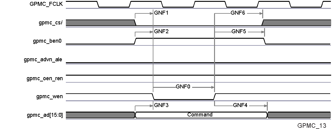
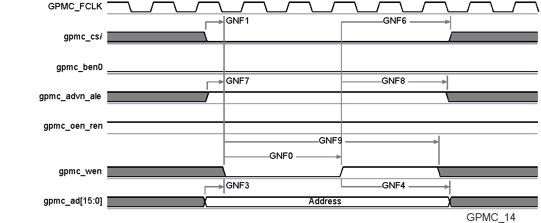
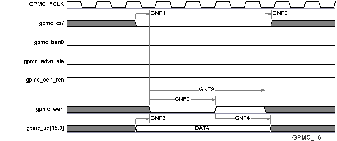
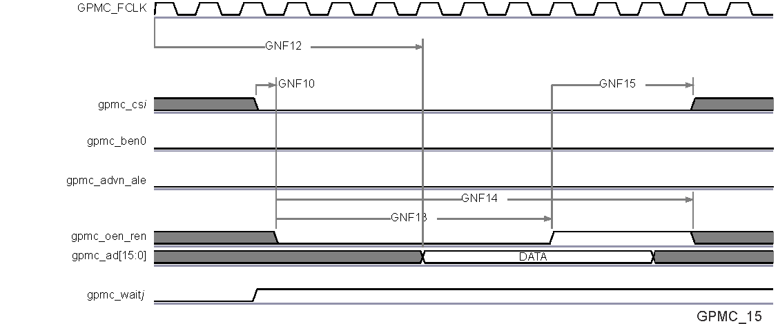
Table 7-31 and Table 7-32 assume testing over the recommended operating conditions and electrical characteristic conditions below (see Figure 7-19, Figure 7-20, Figure 7-21, and Figure 7-22).
Table 7-31 GPMC/NAND Flash Interface Timing Requirements
| NO. | PARAMETER | DESCRIPTION | MIN | MAX | UNIT |
|---|---|---|---|---|---|
| GNF12 | tacc(DAT) | Data maximum access time (GPMC_FCLK Cycles) | J (1) | cycles | |
| - | tsu(DV-OEH) | Setup time, read gpmc_ad[15:0] valid before gpmc_oen_ren high | 1.9 | ns | |
| - | th(OEH-DV) | Hold time, read gpmc_ad[15:0] valid after gpmc_oen_ren high | 1 | ns |
- J = AccessTime * (TimeParaGranularity + 1)
Table 7-32 GPMC/NAND Flash Interface Switching Characteristics
| NO. | PARAMETER | DESCRIPTION | MIN | MAX | UNIT |
|---|---|---|---|---|---|
| - | tr(DO) | Rising time, gpmc_ad[15:0] output data | 0.447 | 4.067 | ns |
| - | tf(DO) | Fallling time, gpmc_ad[15:0] output data | 0.43 | 4.463 | ns |
| GNF0 | tw(nWEV) | Pulse duration, gpmc_wen valid time | A (1) | ns | |
| GNF1 | td(nCSV-nWEV) | Delay time, gpmc_cs[7:0] valid to gpmc_wen valid | B - 2 (2) | B + 4 (2) | ns |
| GNF2 | td(CLEH-nWEV) | Delay time, gpmc_ben[1:0] high to gpmc_wen valid | C - 2 (3) | C + 4 (3) | ns |
| GNF3 | td(nWEV-DV) | Delay time, gpmc_ad[15:0] valid to gpmc_wen valid | D - 2 (4) | D + 4 (4) | ns |
| GNF4 | td(nWEIV-DIV) | Delay time, gpmc_wen invalid to gpmc_ad[15:0] invalid | E - 2 (5) | E + 4 (5) | ns |
| GNF5 | td(nWEIV-CLEIV) | Delay time, gpmc_wen invalid to gpmc_ben[1:0] invalid | F - 2 (6) | F + 4 (6) | ns |
| GNF6 | td(nWEIV-nCSIV) | Delay time, gpmc_wen invalid to gpmc_cs[7:0] invalid | G - 2 (7) | G + 4 (7) | ns |
| GNF7 | td(ALEH-nWEV) | Delay time, gpmc_advn_ale high to gpmc_wen valid | C - 2 (3) | C + 4 (3) | ns |
| GNF8 | td(nWEIV-ALEIV) | Delay time, gpmc_wen invalid to gpmc_advn_ale invalid | F - 2 (6) | F + 4 (6) | ns |
| GNF9 | tc(nWE) | Cycle time, write cycle time | H (8) | ns | |
| GNF10 | td(nCSV-nOEV) | Delay time, gpmc_cs[7:0] valid to gpmc_oen_ren valid | I - 2 (9) | I + 4 (9) | ns |
| GNF13 | tw(nOEV) | Pulse duration, gpmc_oen_ren valid time | K (10) | ns | |
| GNF14 | tc(nOE) | Cycle time, read cycle time | L (11) | ns | |
| GNF15 | td(nOEIV-nCSIV) | Delay time, gpmc_oen_ren invalid to gpmc_cs[7:0] invalid | M - 2 (12) | M + 4 (12) | ns |
- A = (WEOffTime – WEOnTime) * (TimeParaGranularity + 1) * GPMC_FCLK
- B = ((WEOnTime – CSOnTime) * (TimeParaGranularity + 1) + 0.5 * (WEExtraDelay – CSExtraDelay)) * GPMC_FCLK
- C = ((WEOnTime – ADVOnTime) * (TimeParaGranularity + 1) + 0.5 * (WEExtraDelay – ADVExtraDelay)) * GPMC_FCLK
- D = (WEOnTime * (TimeParaGranularity + 1) + 0.5 * WEExtraDelay ) * GPMC_FCLK
- E = (WrCycleTime – WEOffTime * (TimeParaGranularity + 1) – 0.5 * WEExtraDelay ) * GPMC_FCLK
- F = (ADVWrOffTime – WEOffTime * (TimeParaGranularity + 1) + 0.5 * (ADVExtraDelay – WEExtraDelay) * GPMC_FCLK
- G = (CSWrOffTime – WEOffTime * (TimeParaGranularity + 1) + 0.5 * (CSExtraDelay – WEExtraDelay) * GPMC_FCLK
- H = WrCycleTime * (1 + TimeParaGranularity) * GPMC_FCLK
- I = ((OEOffTime + (n – 1) * PageBurstAccessTime – CSOnTime) * (TimeParaGranularity + 1) + 0.5 * (OEExtraDelay – CSExtraDelay)) * GPMC_FCLK
- K = (OEOffTime – OEOnTime) * (1 + TimeParaGranularity) * GPMC_FCLK
- L = RdCycleTime * (1 + TimeParaGranularity) * GPMC_FCLK
- M = (CSRdOffTime – OEOffTime * (TimeParaGranularity + 1) + 0.5 * (CSExtraDelay – OEExtraDelay) * GPMC_FCLK
 Figure 7-19 GPMC / NAND Flash - Command Latch Cycle Timing(1)
 - In gpmc_csi, i = 0 to 7.
 Figure 7-20 GPMC / NAND Flash - Address Latch Cycle Timing(1)
 - In gpmc_csi, i = 0 to 7.
- GNF12 parameter illustrates amount of time required to internally sample input Data. It is expressed in number of GPMC functional clock cycles. From start of read cycle and after GNF12 functional clock cycles, input data will be internally sampled by active functional clock edge. GNF12 value must be stored inside AccessTime register bits field.
- GPMC_FCLK is an internal clock (GPMC functional clock) not provided externally.
- In gpmc_csi, i = 0 to 7. In gpmc_waitj, j = 0 to 1.
 Figure 7-22 GPMC / NAND Flash - Data Write Cycle Timing(1)
 - In gpmc_csi, i = 0 to 7.
NOTE
To configure the desired virtual mode the user must set MODESELECT bit and DELAYMODE bitfield for each corresponding pad control register.
The pad control registers are presented in Table 4-3 and described in Device TRM, Control Module Chapter.
Virtual IO Timings Modes must be used to ensure some IO timings for GPMC. See Table 7-2Modes Summary for a list of IO timings requiring the use of Virtual IO Timings Modes. See Table 7-33Virtual Functions Mapping for GPMC for a definition of the Virtual modes.
Table 7-33 presents the values for DELAYMODE bitfield.
Table 7-33 Virtual Functions Mapping for GPMC
| BALL | BALL NAME | Delay Mode Value | MUXMODE[15:0] | |||||
|---|---|---|---|---|---|---|---|---|
| GPMC_VIRTUAL1 | 0 | 1 | 2 | 3 | 5 | 6 | ||
| M6 | gpmc_ad0 | 11 | gpmc_ad0 | |||||
| M2 | gpmc_ad1 | 11 | gpmc_ad1 | |||||
| L5 | gpmc_ad2 | 11 | gpmc_ad2 | |||||
| M1 | gpmc_ad3 | 11 | gpmc_ad3 | |||||
| L6 | gpmc_ad4 | 11 | gpmc_ad4 | |||||
| L4 | gpmc_ad5 | 11 | gpmc_ad5 | |||||
| L3 | gpmc_ad6 | 11 | gpmc_ad6 | |||||
| L2 | gpmc_ad7 | 11 | gpmc_ad7 | |||||
| L1 | gpmc_ad8 | 11 | gpmc_ad8 | |||||
| K2 | gpmc_ad9 | 11 | gpmc_ad9 | |||||
| J1 | gpmc_ad10 | 11 | gpmc_ad10 | |||||
| J2 | gpmc_ad11 | 11 | gpmc_ad11 | |||||
| H1 | gpmc_ad12 | 11 | gpmc_ad12 | |||||
| J3 | gpmc_ad13 | 11 | gpmc_ad13 | |||||
| H2 | gpmc_ad14 | 11 | gpmc_ad14 | |||||
| H3 | gpmc_ad15 | 11 | gpmc_ad15 | |||||
| R6 | gpmc_a0 | 11 | gpmc_a0 | |||||
| T9 | gpmc_a1 | 11 | gpmc_a1 | |||||
| T6 | gpmc_a2 | 11 | gpmc_a2 | |||||
| T7 | gpmc_a3 | 10 | gpmc_a3 | |||||
| P6 | gpmc_a4 | 10 | gpmc_a4 | |||||
| R9 | gpmc_a5 | 11 | gpmc_a5 | |||||
| R5 | gpmc_a6 | 11 | gpmc_a6 | |||||
| P5 | gpmc_a7 | 11 | gpmc_a7 | |||||
| N7 | gpmc_a8 | 12 | gpmc_a8 | |||||
| R4 | gpmc_a9 | 12 | gpmc_a9 | |||||
| N9 | gpmc_a10 | 12 | gpmc_a10 | |||||
| P9 | gpmc_a11 | 11 | gpmc_a11 | |||||
| P4 | gpmc_a12 | 13 | gpmc_a12 | gpmc_a0 | ||||
| R3 | gpmc_a13 | 12 | gpmc_a13 | |||||
| T2 | gpmc_a14 | 12 | gpmc_a14 | |||||
| U2 | gpmc_a15 | 12 | gpmc_a15 | |||||
| U1 | gpmc_a16 | 12 | gpmc_a16 | |||||
| P3 | gpmc_a17 | 12 | gpmc_a17 | |||||
| R2 | gpmc_a18 | 12 | gpmc_a18 | |||||
| K7 | gpmc_a19 | 11 | gpmc_a19 | gpmc_a13 | ||||
| M7 | gpmc_a20 | 11 | gpmc_a20 | gpmc_a14 | ||||
| J5 | gpmc_a21 | 11 | gpmc_a21 | gpmc_a15 | ||||
| K6 | gpmc_a22 | 11 | gpmc_a22 | gpmc_a16 | ||||
| J7 | gpmc_a23 | 11 | gpmc_a23 | gpmc_a17 | ||||
| J4 | gpmc_a24 | 11 | gpmc_a24 | gpmc_a18 | ||||
| J6 | gpmc_a25 | 11 | gpmc_a25 | gpmc_a19 | ||||
| H4 | gpmc_a26 | 11 | gpmc_a26 | gpmc_a20 | ||||
| H5 | gpmc_a27 | 11 | gpmc_a27 | gpmc_a21 | ||||
| H6 | gpmc_cs1 | 11 | gpmc_cs1 | gpmc_a22 | ||||
| T1 | gpmc_cs0 | 14 | gpmc_cs0 | |||||
| P2 | gpmc_cs2 | 12 | gpmc_cs2 | |||||
| P1 | gpmc_cs3 | 10 | gpmc_cs3 | gpmc_a1 | ||||
| P7 | gpmc_clk | 12 | gpmc_clk | gpmc_cs7 | gpmc_wait1 | |||
| N1 | gpmc_advn_ale | 13 | gpmc_advn_ale | gpmc_cs6 | gpmc_wait1 | gpmc_a2 | gpmc_a23 | |
| M5 | gpmc_oen_ren | 14 | gpmc_oen_ren | |||||
| M3 | gpmc_wen | 14 | gpmc_wen | |||||
| N6 | gpmc_ben0 | 11 | gpmc_ben0 | gpmc_cs4 | ||||
| M4 | gpmc_ben1 | 11 | gpmc_ben1 | gpmc_cs5 | gpmc_a3 | |||
| N2 | gpmc_wait0 | 14 | gpmc_wait0 | |||||
| AG5 | vin1a_d11 | 9 | gpmc_a23 | |||||
| AF2 | vin1a_d12 | 9 | gpmc_a24 | |||||
| AF6 | vin1a_d13 | 9 | gpmc_a25 | |||||
| AF3 | vin1a_d14 | 9 | gpmc_a26 | |||||
| AF4 | vin1a_d15 | 9 | gpmc_a27 | |||||
