JAJSGK9F December 2015 – May 2019 TDA2HF , TDA2HG , TDA2HV , TDA2LF , TDA2SA , TDA2SG , TDA2SX
PRODUCTION DATA.
- 1 デバイスの概要
- 2 改訂履歴
- 3 Device Comparison
-
4 Terminal Configuration and Functions
- 4.1 Terminal Assignment
- 4.2 Ball Characteristics
- 4.3 Multiplexing Characteristics
- 4.4
Signal Descriptions
- 4.4.1 Video Input Port (VIP)
- 4.4.2 Display Subsystem – Video Output Ports
- 4.4.3 Display Subsystem – High-Definition Multimedia Interface (HDMI)
- 4.4.4 External Memory Interface (EMIF)
- 4.4.5 General-Purpose Memory Controller (GPMC)
- 4.4.6 Timers
- 4.4.7 Inter-Integrated Circuit Interface (I2C)
- 4.4.8 Universal Asynchronous Receiver Transmitter (UART)
- 4.4.9 Multichannel Serial Peripheral Interface (McSPI)
- 4.4.10 Quad Serial Peripheral Interface (QSPI)
- 4.4.11 Multichannel Audio Serial Port (McASP)
- 4.4.12 Universal Serial Bus (USB)
- 4.4.13 SATA
- 4.4.14 Peripheral Component Interconnect Express (PCIe)
- 4.4.15 Controller Area Network Interface (DCAN)
- 4.4.16 Ethernet Interface (GMAC_SW)
- 4.4.17 eMMC/SD/SDIO
- 4.4.18 General-Purpose Interface (GPIO)
- 4.4.19 Pulse Width Modulation (PWM) Interface
- 4.4.20 System and Miscellaneous
- 4.4.21 Test Interfaces
-
5 Specifications
- 5.1 Absolute Maximum Ratings
- 5.2 ESD Ratings
- 5.3 Power on Hour (POH) Limits
- 5.4 Recommended Operating Conditions
- 5.5 Operating Performance Points
- 5.6 Power Consumption Summary
- 5.7
Electrical Characteristics
- 5.7.1 LVCMOS DDR DC Electrical Characteristics
- 5.7.2 HDMIPHY DC Electrical Characteristics
- 5.7.3 Dual Voltage LVCMOS I2C DC Electrical Characteristics
- 5.7.4 IQ1833 Buffers DC Electrical Characteristics
- 5.7.5 IHHV1833 Buffers DC Electrical Characteristics
- 5.7.6 LVCMOS OSC Buffers DC Electrical Characteristics
- 5.7.7 BC1833IHHV Buffers DC Electrical Characteristics
- 5.7.8 USBPHY DC Electrical Characteristics
- 5.7.9 Dual Voltage SDIO1833 DC Electrical Characteristics
- 5.7.10 Dual Voltage LVCMOS DC Electrical Characteristics
- 5.7.11 SATAPHY DC Electrical Characteristics
- 5.7.12 PCIEPHY DC Electrical Characteristics
- 5.8 Thermal Resistance Characteristics
- 5.9 Power Supply Sequences
- 6 Clock Specifications
-
7 Timing Requirements and Switching Characteristics
- 7.1 Timing Test Conditions
- 7.2 Interface Clock Specifications
- 7.3 Timing Parameters and Information
- 7.4 Recommended Clock and Control Signal Transition Behavior
- 7.5 Virtual and Manual I/O Timing Modes
- 7.6 Video Input Ports (VIP)
- 7.7 Display Subsystem – Video Output Ports
- 7.8 Display Subsystem – High-Definition Multimedia Interface (HDMI)
- 7.9 External Memory Interface (EMIF)
- 7.10 General-Purpose Memory Controller (GPMC)
- 7.11 Timers
- 7.12 Inter-Integrated Circuit Interface (I2C)
- 7.13 Universal Asynchronous Receiver Transmitter (UART)
- 7.14 Multichannel Serial Peripheral Interface (McSPI)
- 7.15 Quad Serial Peripheral Interface (QSPI)
- 7.16
Multichannel Audio Serial Port (McASP)
- Table 7-45 Timing Requirements for McASP1
- Table 7-46 Timing Requirements for McASP2
- Table 7-47 Timing Requirements for McASP3/4/5/6/7/8
- Table 7-48 Switching Characteristics Over Recommended Operating Conditions for McASP1
- Table 7-49 Switching Characteristics Over Recommended Operating Conditions for McASP2
- Table 7-50 Switching Characteristics Over Recommended Operating Conditions for McASP3/4/5/6/7/8
- 7.17 Universal Serial Bus (USB)
- 7.18 Serial Advanced Technology Attachment (SATA)
- 7.19 Peripheral Component Interconnect Express (PCIe)
- 7.20 Controller Area Network Interface (DCAN)
- 7.21
Ethernet Interface (GMAC_SW)
- 7.21.1
GMAC MII Timings
- Table 7-67 Timing Requirements for miin_rxclk - MII Operation
- Table 7-68 Timing Requirements for miin_txclk - MII Operation
- Table 7-69 Timing Requirements for GMAC MIIn Receive 10/100 Mbit/s
- Table 7-70 Switching Characteristics Over Recommended Operating Conditions for GMAC MIIn Transmit 10/100 Mbits/s
- 7.21.2 GMAC MDIO Interface Timings
- 7.21.3
GMAC RMII Timings
- Table 7-75 Timing Requirements for GMAC REF_CLK - RMII Operation
- Table 7-76 Timing Requirements for GMAC RMIIn Receive
- Table 7-77 Switching Characteristics Over Recommended Operating Conditions for GMAC REF_CLK - RMII Operation
- Table 7-78 Switching Characteristics Over Recommended Operating Conditions for GMAC RMIIn Transmit 10/100 Mbits/s
- 7.21.4
GMAC RGMII Timings
- Table 7-82 Timing Requirements for rgmiin_rxc - RGMIIn Operation
- Table 7-83 Timing Requirements for GMAC RGMIIn Input Receive for 10/100/1000 Mbps
- Table 7-84 Switching Characteristics Over Recommended Operating Conditions for rgmiin_txctl - RGMIIn Operation for 10/100/1000 Mbit/s
- Table 7-85 Switching Characteristics for GMAC RGMIIn Output Transmit for 10/100/1000 Mbps
- 7.21.1
GMAC MII Timings
- 7.22
eMMC/SD/SDIO
- 7.22.1
MMC1—SD Card Interface
- 7.22.1.1 Default speed, 4-bit data, SDR, half-cycle
- 7.22.1.2 High speed, 4-bit data, SDR, half-cycle
- 7.22.1.3 SDR12, 4-bit data, half-cycle
- 7.22.1.4 SDR25, 4-bit data, half-cycle
- 7.22.1.5 UHS-I SDR50, 4-bit data, half-cycle
- 7.22.1.6 UHS-I SDR104, 4-bit data, half-cycle
- 7.22.1.7 UHS-I DDR50, 4-bit data
- 7.22.2 MMC2 — eMMC
- 7.22.3 MMC3 and MMC4—SDIO/SD
- 7.22.1
MMC1—SD Card Interface
- 7.23 General-Purpose Interface (GPIO)
- 7.24 System and Miscellaneous interfaces
- 7.25
Test Interfaces
- 7.25.1
IEEE 1149.1 Standard-Test-Access Port (JTAG)
- 7.25.1.1
JTAG Electrical Data/Timing
- Table 7-134 Timing Requirements for IEEE 1149.1 JTAG
- Table 7-135 Switching Characteristics Over Recommended Operating Conditions for IEEE 1149.1 JTAG
- Table 7-136 Timing Requirements for IEEE 1149.1 JTAG With RTCK
- Table 7-137 Switching Characteristics Over Recommended Operating Conditions for IEEE 1149.1 JTAG With RTCK
- 7.25.1.1
JTAG Electrical Data/Timing
- 7.25.2 Trace Port Interface Unit (TPIU)
- 7.25.1
IEEE 1149.1 Standard-Test-Access Port (JTAG)
-
8 Applications, Implementation, and Layout
- 8.1 Introduction
- 8.2 Power Optimizations
- 8.3 Core Power Domains
- 8.4 Single-Ended Interfaces
- 8.5
Differential Interfaces
- 8.5.1 General Routing Guidelines
- 8.5.2
USB 2.0 Board Design and Layout Guidelines
- 8.5.2.1 Background
- 8.5.2.2
USB PHY Layout Guide
- 8.5.2.2.1 General Routing and Placement
- 8.5.2.2.2
Specific Guidelines for USB PHY Layout
- 8.5.2.2.2.1 Analog, PLL, and Digital Power Supply Filtering
- 8.5.2.2.2.2 Analog, Digital, and PLL Partitioning
- 8.5.2.2.2.3 Board Stackup
- 8.5.2.2.2.4 Cable Connector Socket
- 8.5.2.2.2.5 Clock Routings
- 8.5.2.2.2.6 Crystals/Oscillator
- 8.5.2.2.2.7 DP/DM Trace
- 8.5.2.2.2.8 DP/DM Vias
- 8.5.2.2.2.9 Image Planes
- 8.5.2.2.2.10 JTAG Interface
- 8.5.2.2.2.11 Power Regulators
- 8.5.2.3 Electrostatic Discharge (ESD)
- 8.5.2.4 References
- 8.5.3 USB 3.0 Board Design and Layout Guidelines
- 8.5.4 HDMI Board Design and Layout Guidelines
- 8.5.5 SATA Board Design and Layout Guidelines
- 8.5.6 PCIe Board Design and Layout Guidelines
- 8.6 Clock Routing Guidelines
- 8.7
DDR2/DDR3 Board Design and Layout Guidelines
- 8.7.1 DDR2/DDR3 General Board Layout Guidelines
- 8.7.2 DDR2 Board Design and Layout Guidelines
- 8.7.3
DDR3 Board Design and Layout Guidelines
- 8.7.3.1 Board Designs
- 8.7.3.2 DDR3 EMIFs
- 8.7.3.3 DDR3 Device Combinations
- 8.7.3.4 DDR3 Interface Schematic
- 8.7.3.5 Compatible JEDEC DDR3 Devices
- 8.7.3.6 PCB Stackup
- 8.7.3.7 Placement
- 8.7.3.8 DDR3 Keepout Region
- 8.7.3.9 Bulk Bypass Capacitors
- 8.7.3.10 High-Speed Bypass Capacitors
- 8.7.3.11 Net Classes
- 8.7.3.12 DDR3 Signal Termination
- 8.7.3.13 VREF_DDR Routing
- 8.7.3.14 VTT
- 8.7.3.15 CK and ADDR_CTRL Topologies and Routing Definition
- 8.7.3.16 Data Topologies and Routing Definition
- 8.7.3.17 Routing Specification
- 9 Device and Documentation Support
- 10Mechanical, Packaging, and Orderable Information
パッケージ・オプション
デバイスごとのパッケージ図は、PDF版データシートをご参照ください。
メカニカル・データ(パッケージ|ピン)
- ABC|760
サーマルパッド・メカニカル・データ
発注情報
8.7.3.4.2 16-Bit DDR3 Interface
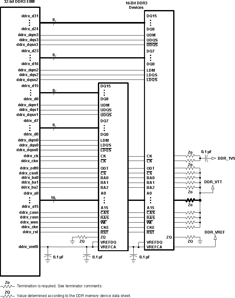
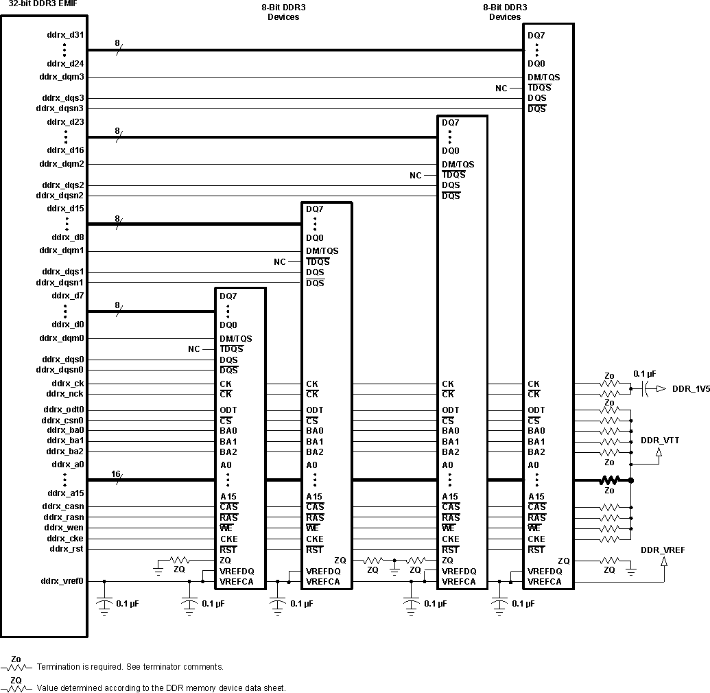
Note that the 16-bit wide interface schematic is practically identical to the 32-bit interface (see Figure 8-58 and Figure 8-59); only the high-word DDR memories are removed and the unused DQS inputs are tied off.
When not using all or part of a DDR interface, the proper method of handling the unused pins is to tie off the ddrx_dqsi pins to ground via a 1k-Ω resistor and to tie off the ddrx_dqsni pins to the corresponding vdds_ddrx supply via a 1k-Ω resistor. This needs to be done for each byte not used. Although these signals have internal pullups and pulldowns, external pullups and pulldowns provide additional protection against external electrical noise causing activity on the signals.
The vdds_ddrx and ddrx_vref0 power supply pins need to be connected to their respective power supplies even if ddrx is not being used. All other DDR interface pins can be left unconnected. Note that the supported modes for use of the DDR EMIF are 32-bits wide, 16-bits wide, or not used.
 Figure 8-58 32-Bit, One-Bank DDR3 Interface Schematic Using Two 16-Bit DDR3 Devices
  Figure 8-59 32-Bit, One-Bank DDR3 Interface Schematic Using Four 8-Bit DDR3 Devices