JAJSGN1F December   2016  – December 2018 TDA2P-ABZ

ADVANCE INFORMATION for pre-production products; subject to change without notice.  

  1. 1デバイスの概要
    1. 1.1 特長
    2. 1.2 アプリケーション
    3. 1.3 概要
    4. 1.4 機能ブロック図
  2. 2改訂履歴
  3. 3Device Comparison
    1. 3.1 Device Comparison Table
    2. 3.2 Related Products
  4. 4Terminal Configuration and Functions
    1. 4.1 Pin Diagram
    2. 4.2 Pin Attributes
    3. 4.3 Signal Descriptions
      1. 4.3.1  VIP
      2. 4.3.2  DSS
      3. 4.3.3  HDMI
      4. 4.3.4  EMIF
      5. 4.3.5  GPMC
      6. 4.3.6  Timers
      7. 4.3.7  I2C
      8. 4.3.8  UART
      9. 4.3.9  McSPI
      10. 4.3.10 QSPI
      11. 4.3.11 McASP
      12. 4.3.12 USB
      13. 4.3.13 SATA
      14. 4.3.14 PCIe
      15. 4.3.15 DCAN and MCAN
      16. 4.3.16 GMAC_SW
      17. 4.3.17 eMMC/SD/SDIO
      18. 4.3.18 GPIO
      19. 4.3.19 PWM
      20. 4.3.20 System and Miscellaneous
        1. 4.3.20.1 Sysboot Interface
        2. 4.3.20.2 PRCM
        3. 4.3.20.3 RTC
        4. 4.3.20.4 SDMA
        5. 4.3.20.5 INTC
        6. 4.3.20.6 Observability
        7. 4.3.20.7 Power Supplies
      21. 4.3.21 Test Interfaces
    4. 4.4 Pin Multiplexing
    5. 4.5 Connections for Unused Pins
  5. 5Specifications
    1. 5.1  Absolute Maximum Ratings
    2. 5.2  ESD Ratings
    3. 5.3  Power-On Hours (POH) Limits
    4. 5.4  Recommended Operating Conditions
    5. 5.5  Operating Performance Points
      1. 5.5.1 AVS and ABB Requirements
      2. 5.5.2 Voltage And Core Clock Specifications
      3. 5.5.3 Maximum Supported Frequency
    6. 5.6  Power Consumption Summary
    7. 5.7  Electrical Characteristics
      1. Table 5-6  LVCMOS DDR DC Electrical Characteristics
      2. Table 5-7  Dual Voltage LVCMOS I2C DC Electrical Characteristics
      3. Table 5-8  IQ1833 Buffers DC Electrical Characteristics
      4. Table 5-9  IHHV1833 Buffers DC Electrical Characteristics
      5. Table 5-10 LVCMOS OSC Buffers DC Electrical Characteristics
      6. Table 5-11 BC1833IHHV Buffers DC Electrical Characteristics
      7. Table 5-12 Dual Voltage SDIO1833 DC Electrical Characteristics
      8. Table 5-13 Dual Voltage LVCMOS DC Electrical Characteristics
      9. 5.7.1      HDMIPHY DC Electrical Characteristics
      10. 5.7.2      SATAPHY DC Electrical Characteristics
      11. 5.7.3      USBPHY DC Electrical Characteristics
      12. 5.7.4      PCIEPHY DC Electrical Characteristics
    8. 5.8  VPP Specifications for One-Time Programmable (OTP) eFuses
      1. Table 5-14 Recommended Operating Conditions for OTP eFuse Programming
      2. 5.8.1      Hardware Requirements
      3. 5.8.2      Programming Sequence
      4. 5.8.3      Impact to Your Hardware Warranty
    9. 5.9  Thermal Resistance Characteristics
      1. 5.9.1 Package Thermal Characteristics
    10. 5.10 Timing Requirements and Switching Characteristics
      1. 5.10.1 Timing Parameters and Information
        1. 5.10.1.1 Parameter Information
          1. 5.10.1.1.1 1.8V and 3.3V Signal Transition Levels
          2. 5.10.1.1.2 1.8V and 3.3V Signal Transition Rates
          3. 5.10.1.1.3 Timing Parameters and Board Routing Analysis
      2. 5.10.2 Interface Clock Specifications
        1. 5.10.2.1 Interface Clock Terminology
        2. 5.10.2.2 Interface Clock Frequency
      3. 5.10.3 Power Supply Sequences
      4. 5.10.4 Clock Specifications
        1. 5.10.4.1 Input Clocks / Oscillators
          1. 5.10.4.1.1 OSC0 External Crystal
          2. 5.10.4.1.2 OSC0 Input Clock
          3. 5.10.4.1.3 Auxiliary Oscillator OSC1 Input Clock
            1. 5.10.4.1.3.1 OSC1 External Crystal
            2. 5.10.4.1.3.2 OSC1 Input Clock
          4. 5.10.4.1.4 RTC Oscillator Input Clock
            1. 5.10.4.1.4.1 RTC Oscillator External Crystal
            2. 5.10.4.1.4.2 RTC Oscillator Input Clock
        2. 5.10.4.2 RC On-die Oscillator Clock
        3. 5.10.4.3 Output Clocks
        4. 5.10.4.4 DPLLs, DLLs
          1. 5.10.4.4.1 DPLL Characteristics
          2. 5.10.4.4.2 DLL Characteristics
          3. 5.10.4.4.3 DPLL and DLL Noise Isolation
      5. 5.10.5 Recommended Clock and Control Signal Transition Behavior
      6. 5.10.6 Peripherals
        1. 5.10.6.1  Timing Test Conditions
        2. 5.10.6.2  Virtual and Manual I/O Timing Modes
        3. 5.10.6.3  VIP
        4. 5.10.6.4  DSS
        5. 5.10.6.5  HDMI
        6. 5.10.6.6  EMIF
        7. 5.10.6.7  GPMC
          1. 5.10.6.7.1 GPMC/NOR Flash Interface Synchronous Timing
          2. 5.10.6.7.2 GPMC/NOR Flash Interface Asynchronous Timing
          3. 5.10.6.7.3 GPMC/NAND Flash Interface Asynchronous Timing
        8. 5.10.6.8  Timers
        9. 5.10.6.9  I2C
          1. Table 5-63 Timing Requirements for I2C Input Timings
          2. Table 5-64 Timing Requirements for I2C HS-Mode (I2C3/4/5 Only)
          3. Table 5-65 Switching Characteristics Over Recommended Operating Conditions for I2C Output Timings
        10. 5.10.6.10 UART
          1. Table 5-66 Timing Requirements for UART
          2. Table 5-67 Switching Characteristics Over Recommended Operating Conditions for UART
        11. 5.10.6.11 McSPI
        12. 5.10.6.12 QSPI
        13. 5.10.6.13 McASP
          1. Table 5-74 Timing Requirements for McASP1
          2. Table 5-75 Timing Requirements for McASP2
          3. Table 5-76 Timing Requirements for McASP3/4/5/6/7/8
          4. Table 5-77 Switching Characteristics Over Recommended Operating Conditions for McASP1
          5. Table 5-78 Switching Characteristics Over Recommended Operating Conditions for McASP2
          6. Table 5-79 Switching Characteristics Over Recommended Operating Conditions for McASP3/4/5/6/7/8
        14. 5.10.6.14 USB
          1. 5.10.6.14.1 USB1 DRD PHY
          2. 5.10.6.14.2 USB2 PHY
          3. 5.10.6.14.3 USB3 and USB4 DRD ULPI—SDR—Slave Mode—12-pin Mode
        15. 5.10.6.15 SATA
        16. 5.10.6.16 PCIe
        17. 5.10.6.17 CAN
          1. 5.10.6.17.1 DCAN
          2. 5.10.6.17.2 MCAN-FD
          3. Table 5-94  Timing Requirements for CANx Receive
          4. Table 5-95  Switching Characteristics Over Recommended Operating Conditions for CANx Transmit
        18. 5.10.6.18 GMAC_SW
          1. 5.10.6.18.1 GMAC MII Timings
            1. Table 5-96 Timing Requirements for miin_rxclk - MII Operation
            2. Table 5-97 Timing Requirements for miin_txclk - MII Operation
            3. Table 5-98 Timing Requirements for GMAC MIIn Receive 10/100 Mbit/s
            4. Table 5-99 Switching Characteristics Over Recommended Operating Conditions for GMAC MIIn Transmit 10/100 Mbits/s
          2. 5.10.6.18.2 GMAC MDIO Interface Timings
          3. 5.10.6.18.3 GMAC RMII Timings
            1. Table 5-104 Timing Requirements for GMAC REF_CLK - RMII Operation
            2. Table 5-105 Timing Requirements for GMAC RMIIn Receive
            3. Table 5-106 Switching Characteristics Over Recommended Operating Conditions for GMAC REF_CLK - RMII Operation
            4. Table 5-107 Switching Characteristics Over Recommended Operating Conditions for GMAC RMIIn Transmit 10/100 Mbits/s
          4. 5.10.6.18.4 GMAC RGMII Timings
            1. Table 5-111 Timing Requirements for rgmiin_rxc - RGMIIn Operation
            2. Table 5-112 Timing Requirements for GMAC RGMIIn Input Receive for 10/100/1000 Mbps
            3. Table 5-113 Switching Characteristics Over Recommended Operating Conditions for rgmiin_txctl - RGMIIn Operation for 10/100/1000 Mbit/s
            4. Table 5-114 Switching Characteristics for GMAC RGMIIn Output Transmit for 10/100/1000 Mbps
        19. 5.10.6.19 eMMC/SD/SDIO
          1. 5.10.6.19.1 MMC1—SD Card Interface
            1. 5.10.6.19.1.1 Default speed, 4-bit data, SDR, half-cycle
            2. 5.10.6.19.1.2 High speed, 4-bit data, SDR, half-cycle
            3. 5.10.6.19.1.3 SDR12, 4-bit data, half-cycle
            4. 5.10.6.19.1.4 SDR25, 4-bit data, half-cycle
            5. 5.10.6.19.1.5 UHS-I SDR50, 4-bit data, half-cycle
            6. 5.10.6.19.1.6 UHS-I SDR104, 4-bit data, half-cycle
            7. 5.10.6.19.1.7 UHS-I DDR50, 4-bit data
          2. 5.10.6.19.2 MMC2 — eMMC
            1. 5.10.6.19.2.1 Standard JC64 SDR, 8-bit data, half cycle
            2. 5.10.6.19.2.2 High-Speed JC64 SDR, 8-bit data, half cycle
            3. 5.10.6.19.2.3 High-Speed HS200 JC64 SDR, 8-bit data, half cycle
            4. 5.10.6.19.2.4 High-Speed JC64 DDR, 8-bit data
          3. 5.10.6.19.3 MMC3 and MMC4—SDIO/SD
            1. 5.10.6.19.3.1 MMC3 and MMC4, SD Default Speed
            2. 5.10.6.19.3.2 MMC3 and MMC4, SD High Speed
            3. 5.10.6.19.3.3 MMC3 and MMC4, SD and SDIO SDR12 Mode
            4. 5.10.6.19.3.4 MMC3 and MMC4, SD SDR25 Mode
            5. 5.10.6.19.3.5 MMC3 SDIO High-Speed UHS-I SDR50 Mode, Half Cycle
        20. 5.10.6.20 GPIO
        21. 5.10.6.21 System and Miscellaneous interfaces
      7. 5.10.7 Emulation and Debug Subsystem
        1. 5.10.7.1 JTAG
          1. 5.10.7.1.1 JTAG Electrical Data/Timing
            1. Table 5-163 Timing Requirements for IEEE 1149.1 JTAG
            2. Table 5-164 Switching Characteristics Over Recommended Operating Conditions for IEEE 1149.1 JTAG
            3. Table 5-165 Timing Requirements for IEEE 1149.1 JTAG With RTCK
            4. Table 5-166 Switching Characteristics Over Recommended Operating Conditions for IEEE 1149.1 JTAG With RTCK
        2. 5.10.7.2 Trace Port Interface Unit (TPIU)
          1. 5.10.7.2.1 TPIU PLL DDR Mode
  6. 6Detailed Description
    1. 6.1  Description
    2. 6.2  Functional Block Diagram
    3. 6.3  MPU
    4. 6.4  DSP Subsystem
    5. 6.5  ISS
    6. 6.6  IVA
    7. 6.7  EVE
    8. 6.8  IPU
    9. 6.9  VPE
    10. 6.10 GPU
    11. 6.11 Memory Subsystem
      1. 6.11.1 EMIF
      2. 6.11.2 GPMC
      3. 6.11.3 ELM
      4. 6.11.4 OCMC
    12. 6.12 Interprocessor Communication
      1. 6.12.1 Mailbox
      2. 6.12.2 Spinlock
    13. 6.13 Interrupt Controller
    14. 6.14 EDMA
    15. 6.15 Peripherals
      1. 6.15.1  VIP
      2. 6.15.2  DSS
      3. 6.15.3  Timers
      4. 6.15.4  I2C
      5. 6.15.5  UART
        1. 6.15.5.1 UART Features
        2. 6.15.5.2 IrDA Features
        3. 6.15.5.3 CIR Features
      6. 6.15.6  McSPI
      7. 6.15.7  QSPI
      8. 6.15.8  McASP
      9. 6.15.9  USB
      10. 6.15.10 SATA
      11. 6.15.11 PCIe
      12. 6.15.12 CAN
      13. 6.15.13 GMAC_SW
      14. 6.15.14 eMMC/SD/SDIO
      15. 6.15.15 GPIO
      16. 6.15.16 ePWM
      17. 6.15.17 eCAP
      18. 6.15.18 eQEP
    16. 6.16 On-Chip Debug
  7. 7Applications, Implementation, and Layout
    1. 7.1 Introduction
      1. 7.1.1 Initial Requirements and Guidelines
    2. 7.2 Power Optimizations
      1. 7.2.1 Step 1: PCB Stack-up
      2. 7.2.2 Step 2: Physical Placement
      3. 7.2.3 Step 3: Static Analysis
        1. 7.2.3.1 PDN Resistance and IR Drop
      4. 7.2.4 Step 4: Frequency Analysis
      5. 7.2.5 System ESD Generic Guidelines
        1. 7.2.5.1 System ESD Generic PCB Guideline
        2. 7.2.5.2 Miscellaneous EMC Guidelines to Mitigate ESD Immunity
      6. 7.2.6 EMI / EMC Issues Prevention
        1. 7.2.6.1 Signal Bandwidth
        2. 7.2.6.2 Signal Routing
          1. 7.2.6.2.1 Signal Routing—Sensitive Signals and Shielding
          2. 7.2.6.2.2 Signal Routing—Outer Layer Routing
        3. 7.2.6.3 Ground Guidelines
          1. 7.2.6.3.1 PCB Outer Layers
          2. 7.2.6.3.2 Metallic Frames
          3. 7.2.6.3.3 Connectors
          4. 7.2.6.3.4 Guard Ring on PCB Edges
          5. 7.2.6.3.5 Analog and Digital Ground
    3. 7.3 Core Power Domains
      1. 7.3.1 General Constraints and Theory
      2. 7.3.2 Voltage Decoupling
      3. 7.3.3 Static PDN Analysis
      4. 7.3.4 Dynamic PDN Analysis
      5. 7.3.5 Power Supply Mapping
      6. 7.3.6 DPLL Voltage Requirement
      7. 7.3.7 Loss of Input Power Event
      8. 7.3.8 Example PCB Design
        1. 7.3.8.1 Example Stack-up
        2. 7.3.8.2 vdd_mpu Example Analysis
    4. 7.4 Single-Ended Interfaces
      1. 7.4.1 General Routing Guidelines
      2. 7.4.2 QSPI Board Design and Layout Guidelines
    5. 7.5 Differential Interfaces
      1. 7.5.1 General Routing Guidelines
      2. 7.5.2 USB 2.0 Board Design and Layout Guidelines
        1. 7.5.2.1 Background
        2. 7.5.2.2 USB PHY Layout Guide
          1. 7.5.2.2.1 General Routing and Placement
          2. 7.5.2.2.2 Specific Guidelines for USB PHY Layout
            1. 7.5.2.2.2.1  Analog, PLL, and Digital Power Supply Filtering
            2. 7.5.2.2.2.2  Analog, Digital, and PLL Partitioning
            3. 7.5.2.2.2.3  Board Stackup
            4. 7.5.2.2.2.4  Cable Connector Socket
            5. 7.5.2.2.2.5  Clock Routings
            6. 7.5.2.2.2.6  Crystals/Oscillator
            7. 7.5.2.2.2.7  DP/DM Trace
            8. 7.5.2.2.2.8  DP/DM Vias
            9. 7.5.2.2.2.9  Image Planes
            10. 7.5.2.2.2.10 JTAG Interface
            11. 7.5.2.2.2.11 Power Regulators
        3. 7.5.2.3 Electrostatic Discharge (ESD)
          1. 7.5.2.3.1 IEC ESD Stressing Test
            1. 7.5.2.3.1.1 Test Mode
            2. 7.5.2.3.1.2 Air Discharge Mode
            3. 7.5.2.3.1.3 Test Type
          2. 7.5.2.3.2 TI Component Level IEC ESD Test
          3. 7.5.2.3.3 Construction of a Custom USB Connector
          4. 7.5.2.3.4 ESD Protection System Design Consideration
        4. 7.5.2.4 References
      3. 7.5.3 USB 3.0 Board Design and Layout Guidelines
        1. 7.5.3.1 USB 3.0 interface introduction
        2. 7.5.3.2 USB 3.0 General routing rules
      4. 7.5.4 HDMI Board Design and Layout Guidelines
        1. 7.5.4.1 HDMI Interface Schematic
        2. 7.5.4.2 TMDS General Routing Guidelines
        3. 7.5.4.3 TPD5S115
        4. 7.5.4.4 HDMI ESD Protection Device (Required)
        5. 7.5.4.5 PCB Stackup Specifications
        6. 7.5.4.6 Grounding
      5. 7.5.5 SATA Board Design and Layout Guidelines
        1. 7.5.5.1 SATA Interface Schematic
        2. 7.5.5.2 Compatible SATA Components and Modes
        3. 7.5.5.3 PCB Stackup Specifications
        4. 7.5.5.4 Routing Specifications
      6. 7.5.6 PCIe Board Design and Layout Guidelines
        1. 7.5.6.1 PCIe Connections and Interface Compliance
          1. 7.5.6.1.1 Coupling Capacitors
          2. 7.5.6.1.2 Polarity Inversion
        2. 7.5.6.2 Non-standard PCIe connections
          1. 7.5.6.2.1 PCB Stackup Specifications
          2. 7.5.6.2.2 Routing Specifications
            1. 7.5.6.2.2.1 Impedance
            2. 7.5.6.2.2.2 Differential Coupling
            3. 7.5.6.2.2.3 Pair Length Matching
        3. 7.5.6.3 LJCB_REFN/P Connections
    6. 7.6 Clock Routing Guidelines
      1. 7.6.1 32-kHz Oscillator Routing
      2. 7.6.2 Oscillator Ground Connection
    7. 7.7 DDR2/DDR3 Board Design and Layout Guidelines
      1. 7.7.1 DDR2/DDR3 General Board Layout Guidelines
      2. 7.7.2 DDR2 Board Design and Layout Guidelines
        1. 7.7.2.1 Board Designs
        2. 7.7.2.2 DDR2 Interface
          1. 7.7.2.2.1  DDR2 Interface Schematic
          2. 7.7.2.2.2  Compatible JEDEC DDR2 Devices
          3. 7.7.2.2.3  PCB Stackup
          4. 7.7.2.2.4  Placement
          5. 7.7.2.2.5  DDR2 Keepout Region
          6. 7.7.2.2.6  Bulk Bypass Capacitors
          7. 7.7.2.2.7  High-Speed Bypass Capacitors
          8. 7.7.2.2.8  Net Classes
          9. 7.7.2.2.9  DDR2 Signal Termination
          10. 7.7.2.2.10 VREF Routing
        3. 7.7.2.3 DDR2 CK and ADDR_CTRL Routing
      3. 7.7.3 DDR3 Board Design and Layout Guidelines
        1. 7.7.3.1  Board Designs
        2. 7.7.3.2  DDR3 EMIF
        3. 7.7.3.3  DDR3 Device Combinations
        4. 7.7.3.4  DDR3 Interface Schematic
          1. 7.7.3.4.1 32-Bit DDR3 Interface
          2. 7.7.3.4.2 16-Bit DDR3 Interface
        5. 7.7.3.5  Compatible JEDEC DDR3 Devices
        6. 7.7.3.6  PCB Stackup
        7. 7.7.3.7  Placement
        8. 7.7.3.8  DDR3 Keepout Region
        9. 7.7.3.9  Bulk Bypass Capacitors
        10. 7.7.3.10 High-Speed Bypass Capacitors
          1. 7.7.3.10.1 Return Current Bypass Capacitors
        11. 7.7.3.11 Net Classes
        12. 7.7.3.12 DDR3 Signal Termination
        13. 7.7.3.13 VREF_DDR Routing
        14. 7.7.3.14 VTT
        15. 7.7.3.15 CK and ADDR_CTRL Topologies and Routing Definition
          1. 7.7.3.15.1 Four DDR3 Devices
            1. 7.7.3.15.1.1 CK and ADDR_CTRL Topologies, Four DDR3 Devices
            2. 7.7.3.15.1.2 CK and ADDR_CTRL Routing, Four DDR3 Devices
          2. 7.7.3.15.2 Two DDR3 Devices
            1. 7.7.3.15.2.1 CK and ADDR_CTRL Topologies, Two DDR3 Devices
            2. 7.7.3.15.2.2 CK and ADDR_CTRL Routing, Two DDR3 Devices
          3. 7.7.3.15.3 One DDR3 Device
            1. 7.7.3.15.3.1 CK and ADDR_CTRL Topologies, One DDR3 Device
            2. 7.7.3.15.3.2 CK and ADDR/CTRL Routing, One DDR3 Device
        16. 7.7.3.16 Data Topologies and Routing Definition
          1. 7.7.3.16.1 DQS and DQ/DM Topologies, Any Number of Allowed DDR3 Devices
          2. 7.7.3.16.2 DQS and DQ/DM Routing, Any Number of Allowed DDR3 Devices
        17. 7.7.3.17 Routing Specification
          1. 7.7.3.17.1 CK and ADDR_CTRL Routing Specification
          2. 7.7.3.17.2 DQS and DQ Routing Specification
  8. 8Device and Documentation Support
    1. 8.1 Device Nomenclature and Orderable Information
      1. 8.1.1 Standard Package Symbolization
      2. 8.1.2 Device Naming Convention
    2. 8.2 Tools and Software
    3. 8.3 Documentation Support
      1. 8.3.1 FCC Warning
      2. 8.3.2 Information About Cautions and Warnings
    4. 8.4 Receiving Notification of Documentation Updates
    5. 8.5 Community Resources
    6. 8.6 商標
    7. 8.7 静電気放電に関する注意事項
    8. 8.8 Export Control Notice
    9. 8.9 Glossary
  9. 9Mechanical Packaging Information
    1. 9.1 Mechanical Data

パッケージ・オプション

メカニカル・データ(パッケージ|ピン)
サーマルパッド・メカニカル・データ
発注情報

Step 2: Physical Placement

A critical step in designing an optimized PDN is that proper care must be taken to making sure that the initial floor planning of the PCB layout is done with good power integrity design guidelines in mind. The following points are important for optimizing a PCB’s PDN:

  • Minimizing the physical distance between power sources and key high load components is the first step toward optimization. Placing source and load components on the same side of the PCB is desirable. This will minimize via inductance impact for high current loads and steps
  • External trace routing between components must be as wide as possible. The wider the traces, the lower the DC resistance and consequently the lower the static IR drop.
  • Whenever possible for the internal layers (routing and plane), wide traces and copper area fills are preferred for PDN layout. The routing of power nets in plane provide for more interplane capacitance and improved high frequency performance of the PDN.
  • Whenever possible, use a via to component pin/pad ratio of 1:1 or better (i.e. especially decoupling capacitors, power inductors and current sensing resistors). Do not share vias among multiple capacitors for connecting power supply and ground planes.
  • Placement of vias must be as close as possible or even within a component’s solder pad if the PCB technology you are using provides this capability.
  • Figure 7-4 shows an example of acceptable width for power net routing but with poor via placement.
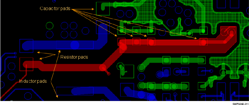
    TDA2P-ABZ SWPS040-211.gifFigure 7-4 Poor Via Assignment for PDN

    Figure 7-5 shows an improved power net routing with better via assignment and placement, respectively.
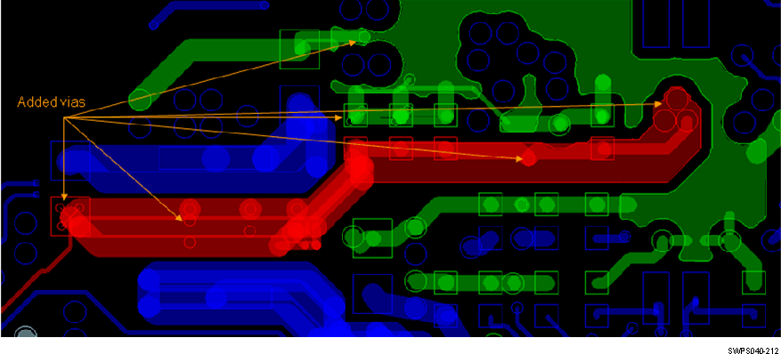
    TDA2P-ABZ SWPS040-212.gifFigure 7-5 Improved Via Assignment for PDN
  • To avoid any “ampacity” issue – maximum current-carrying capacity of each transitional via should be evaluated to determine the appropriate number of vias required to connect components.
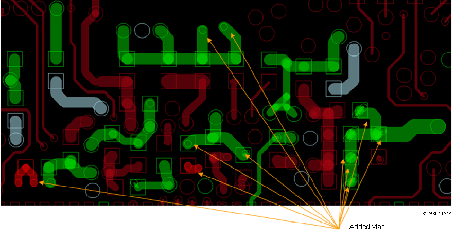
  • Figure 7-6 and Figure 7-7 show examples of “via starvation” on a power net transitioning from top routing layer to internal layers and the improved layout, respectively. Adding vias to bring the “via-to-pad” ratio to 1:1 will improve PDN performance.
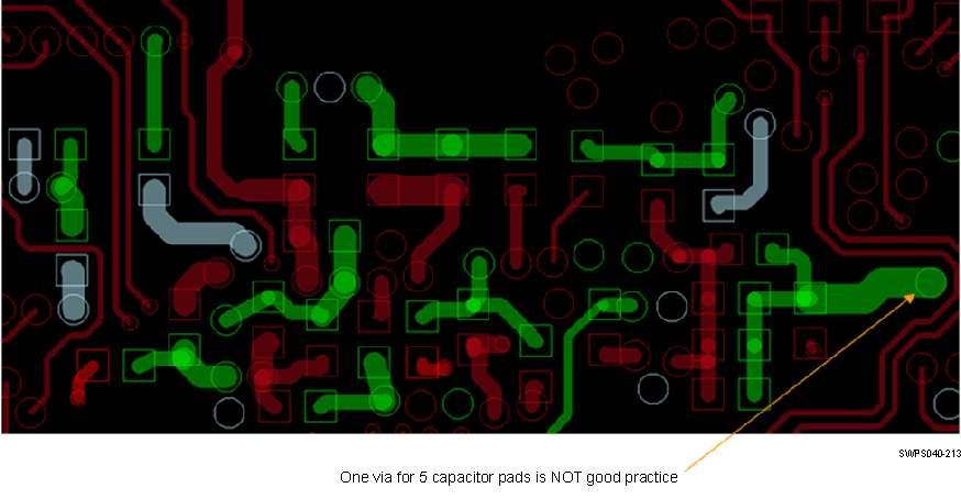
    TDA2P-ABZ SWPS040-213.gifFigure 7-6 Via Starvation
    TDA2P-ABZ SWPS040-214.gifFigure 7-7 Improved Layout With More Transitional Vias
  • For noise sensitive power supplies (i.e. Phase Lock-Loops, analog signals like audio and video), a Gnd shield can be used to isolate coplanar supplies that may have high step currents or high frequency switching transitions from coupling into low-noise supplies.
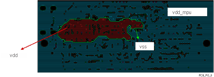
TDA2P-ABZ VAYU_PCB_PO_8.gifFigure 7-8 Coplanar Shielding of Power Net Using Ground Guard-band