JAJSE41G June 2016 – March 2019 TDA3LA , TDA3LX , TDA3MA , TDA3MD , TDA3MV
PRODUCTION DATA.
- 1 デバイスの概要
- 2 改訂履歴
- 3 Device Comparison
-
4 Terminal Configuration and Functions
- 4.1 Terminal Assignment
- 4.2 Ball Characteristics
- 4.3 Multiplexing Characteristics
- 4.4
Signal Descriptions
- 4.4.1 Video Input Ports (VIP)
- 4.4.2 Display Subsystem – Video Output Ports
- 4.4.3 Digital-to-Analog Converter (SD_DAC)
- 4.4.4 Embedded 8 channel Analog-To-Digital Converter (ADC)
- 4.4.5 Camera Control
- 4.4.6 Camera Parallel Interface (CPI)
- 4.4.7 Imaging Subsystem (ISS)
- 4.4.8 External Memory Interface (EMIF)
- 4.4.9 General-Purpose Memory Controller (GPMC)
- 4.4.10 Timers
- 4.4.11 Inter-Integrated Circuit Interface (I2C)
- 4.4.12 Universal Asynchronous Receiver Transmitter (UART)
- 4.4.13 Multichannel Serial Peripheral Interface (McSPI)
- 4.4.14 Quad Serial Peripheral Interface (QSPI)
- 4.4.15 Multichannel Audio Serial Port (McASP)
- 4.4.16 Controller Area Network Interface (DCAN and MCAN)
- 4.4.17 Ethernet Interface (GMAC_SW)
- 4.4.18 SDIO Controller
- 4.4.19 General-Purpose Interface (GPIO)
- 4.4.20 Pulse Width Modulation (PWM) Interface
- 4.4.21 Test Interfaces
- 4.4.22 System and Miscellaneous
- 4.4.23 Power Supplies
-
5 Specifications
- 5.1 Absolute Maximum Ratings
- 5.2 ESD Ratings
- 5.4 Operating Performance Points
- 5.5 Power Consumption Summary
- 5.6
Electrical Characteristics
- 5.6.1 LVCMOS DDR DC Electrical Characteristics
- 5.6.2 Dual Voltage LVCMOS I2C DC Electrical Characteristics
- 5.6.3 IQ1833 Buffers DC Electrical Characteristics
- 5.6.4 IHHV1833 Buffers DC Electrical Characteristics
- 5.6.5 LVCMOS Analog OSC Buffers DC Electrical Characteristics
- 5.6.6 LVCMOS CSI2 DC Electrical Characteristics
- 5.6.7 Dual Voltage LVCMOS DC Electrical Characteristics
- 5.7 Thermal Characteristics
- 5.8 Analog-to-Digital ADC Subsystem Electrical Specifications
- 5.9 Power Supply Sequences
- 6 Clock Specifications
-
7 Timing Requirements and Switching Characteristics
- 7.1 Timing Test Conditions
- 7.2 Interface Clock Specifications
- 7.3 Timing Parameters and Information
- 7.4 Recommended Clock and Control Signal Transition Behavior
- 7.5 Video Input Ports (VIP)
- 7.6 Display Subsystem – Video Output Ports
- 7.7 Imaging Subsystem (ISS)
- 7.8 External Memory Interface (EMIF)
- 7.9 General-Purpose Memory Controller (GPMC)
- 7.10 General-Purpose Timers
- 7.11 Inter-Integrated Circuit Interface (I2C)
- 7.12 Universal Asynchronous Receiver Transmitter (UART)
- 7.13 Multichannel Serial Peripheral Interface (McSPI)
- 7.14 Quad Serial Peripheral Interface (QSPI)
- 7.15
Multichannel Audio Serial Port (McASP)
- Table 7-26 Timing Requirements for McASP1
- Table 7-27 Timing Requirements for McASP2
- Table 7-28 Timing Requirements for McASP3
- Table 7-29 Switching Characteristics Over Recommended Operating Conditions for McASP1
- Table 7-30 Switching Characteristics Over Recommended Operating Conditions for McASP2
- Table 7-31 Switching Characteristics Over Recommended Operating Conditions for McASP3
- 7.16 Controller Area Network Interface (DCAN and MCAN)
- 7.17
Ethernet Interface (GMAC_SW)
- 7.17.1 GMAC MDIO Interface Timings
- 7.17.2
GMAC RGMII Timings
- Table 7-39 Timing Requirements for rgmiin_rxc - RGMIIn Operation
- Table 7-40 Timing Requirements for GMAC RGMIIn Input Receive for 10/100/1000 Mbps
- Table 7-41 Switching Characteristics Over Recommended Operating Conditions for rgmiin_txctl - RGMIIn Operation for 10/100/1000 Mbit/s
- Table 7-42 Switching Characteristics for GMAC RGMIIn Output Transmit for 10/100/1000 Mbps
- 7.18 SDIO Controller
- 7.19 General-Purpose Interface (GPIO)
- 7.20
Test Interfaces
- 7.20.1
JTAG Electrical Data/Timing
- Table 7-53 Timing Requirements for IEEE 1149.1 JTAG
- Table 7-54 Switching Characteristics Over Recommended Operating Conditions for IEEE 1149.1 JTAG
- Table 7-55 Timing Requirements for IEEE 1149.1 JTAG With RTCK
- Table 7-56 Switching Characteristics Over Recommended Operating Conditions for IEEE 1149.1 JTAG With RTCK
- 7.20.2 Trace Port Interface Unit (TPIU)
- 7.20.1
JTAG Electrical Data/Timing
-
8 Applications, Implementation, and Layout
- 8.1 Introduction
- 8.2 Power Optimizations
- 8.3 Core Power Domains
- 8.4 Single-Ended Interfaces
- 8.5 Differential Interfaces
- 8.6 Clock Routing Guidelines
- 8.7 LPDDR2 Board Design and Layout Guidelines
- 8.8 DDR2 Board Design and Layout Guidelines
- 8.9
DDR3 Board Design and Layout Guidelines
- 8.9.1 DDR3 General Board Layout Guidelines
- 8.9.2
DDR3 Board Design and Layout Guidelines
- 8.9.2.1 Board Designs
- 8.9.2.2 DDR3 Device Combinations
- 8.9.2.3 DDR3 Interface Schematic
- 8.9.2.4 Compatible JEDEC DDR3 Devices
- 8.9.2.5 PCB Stackup
- 8.9.2.6 Placement
- 8.9.2.7 DDR3 Keepout Region
- 8.9.2.8 Bulk Bypass Capacitors
- 8.9.2.9 High-Speed Bypass Capacitors
- 8.9.2.10 Net Classes
- 8.9.2.11 DDR3 Signal Termination
- 8.9.2.12 VTT
- 8.9.2.13 CK and ADDR_CTRL Topologies and Routing Definition
- 8.9.2.14 Data Topologies and Routing Definition
- 8.9.2.15 Routing Specification
- 8.10 CVIDEO/SD-DAC Guidelines and Electrical Data/Timing
- 9 Device and Documentation Support
- 10Mechanical, Packaging, and Orderable Information
パッケージ・オプション
デバイスごとのパッケージ図は、PDF版データシートをご参照ください。
メカニカル・データ(パッケージ|ピン)
- ABF|367
サーマルパッド・メカニカル・データ
発注情報
8.2.6.3.4 Guard Ring on PCB Edges
The major advantage of a multilayer PCB with ground-plane is the ground return path below each and every signal or power trace.
As shown in Figure 8-12 the field lines of the signal return to PCB ground as long as an infinite ground is available.
Traces near the PCB-edges do not have this infinite ground and therefore may radiate more than the others. Thus, signals (clocks) or power traces (core power) identified to be critical must not be routed in the vicinity of PCB edges, or, if not avoidable, must be accompanied by a guard ring on the PCB edge.
 Figure 8-12 Field Lines of a Signal Above Ground
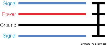
  Figure 8-13 Guard Ring Routing
 The intention of the guard ring is that HF-energy, that otherwise would have been emitted from the PCB edge, is reflected back into the board where it partially will be absorbed. For this purpose ground traces on the borders of all layers (including power layer) must be applied as shown in Figure 8-13.
As these traces must have the same (HF–) potential as the ground plane they must be connected to the ground plane at least every 10 mm.