JAJSE41G June 2016 – March 2019 TDA3LA , TDA3LX , TDA3MA , TDA3MD , TDA3MV
PRODUCTION DATA.
- 1 デバイスの概要
- 2 改訂履歴
- 3 Device Comparison
-
4 Terminal Configuration and Functions
- 4.1 Terminal Assignment
- 4.2 Ball Characteristics
- 4.3 Multiplexing Characteristics
- 4.4
Signal Descriptions
- 4.4.1 Video Input Ports (VIP)
- 4.4.2 Display Subsystem – Video Output Ports
- 4.4.3 Digital-to-Analog Converter (SD_DAC)
- 4.4.4 Embedded 8 channel Analog-To-Digital Converter (ADC)
- 4.4.5 Camera Control
- 4.4.6 Camera Parallel Interface (CPI)
- 4.4.7 Imaging Subsystem (ISS)
- 4.4.8 External Memory Interface (EMIF)
- 4.4.9 General-Purpose Memory Controller (GPMC)
- 4.4.10 Timers
- 4.4.11 Inter-Integrated Circuit Interface (I2C)
- 4.4.12 Universal Asynchronous Receiver Transmitter (UART)
- 4.4.13 Multichannel Serial Peripheral Interface (McSPI)
- 4.4.14 Quad Serial Peripheral Interface (QSPI)
- 4.4.15 Multichannel Audio Serial Port (McASP)
- 4.4.16 Controller Area Network Interface (DCAN and MCAN)
- 4.4.17 Ethernet Interface (GMAC_SW)
- 4.4.18 SDIO Controller
- 4.4.19 General-Purpose Interface (GPIO)
- 4.4.20 Pulse Width Modulation (PWM) Interface
- 4.4.21 Test Interfaces
- 4.4.22 System and Miscellaneous
- 4.4.23 Power Supplies
-
5 Specifications
- 5.1 Absolute Maximum Ratings
- 5.2 ESD Ratings
- 5.4 Operating Performance Points
- 5.5 Power Consumption Summary
- 5.6
Electrical Characteristics
- 5.6.1 LVCMOS DDR DC Electrical Characteristics
- 5.6.2 Dual Voltage LVCMOS I2C DC Electrical Characteristics
- 5.6.3 IQ1833 Buffers DC Electrical Characteristics
- 5.6.4 IHHV1833 Buffers DC Electrical Characteristics
- 5.6.5 LVCMOS Analog OSC Buffers DC Electrical Characteristics
- 5.6.6 LVCMOS CSI2 DC Electrical Characteristics
- 5.6.7 Dual Voltage LVCMOS DC Electrical Characteristics
- 5.7 Thermal Characteristics
- 5.8 Analog-to-Digital ADC Subsystem Electrical Specifications
- 5.9 Power Supply Sequences
- 6 Clock Specifications
-
7 Timing Requirements and Switching Characteristics
- 7.1 Timing Test Conditions
- 7.2 Interface Clock Specifications
- 7.3 Timing Parameters and Information
- 7.4 Recommended Clock and Control Signal Transition Behavior
- 7.5 Video Input Ports (VIP)
- 7.6 Display Subsystem – Video Output Ports
- 7.7 Imaging Subsystem (ISS)
- 7.8 External Memory Interface (EMIF)
- 7.9 General-Purpose Memory Controller (GPMC)
- 7.10 General-Purpose Timers
- 7.11 Inter-Integrated Circuit Interface (I2C)
- 7.12 Universal Asynchronous Receiver Transmitter (UART)
- 7.13 Multichannel Serial Peripheral Interface (McSPI)
- 7.14 Quad Serial Peripheral Interface (QSPI)
- 7.15
Multichannel Audio Serial Port (McASP)
- Table 7-26 Timing Requirements for McASP1
- Table 7-27 Timing Requirements for McASP2
- Table 7-28 Timing Requirements for McASP3
- Table 7-29 Switching Characteristics Over Recommended Operating Conditions for McASP1
- Table 7-30 Switching Characteristics Over Recommended Operating Conditions for McASP2
- Table 7-31 Switching Characteristics Over Recommended Operating Conditions for McASP3
- 7.16 Controller Area Network Interface (DCAN and MCAN)
- 7.17
Ethernet Interface (GMAC_SW)
- 7.17.1 GMAC MDIO Interface Timings
- 7.17.2
GMAC RGMII Timings
- Table 7-39 Timing Requirements for rgmiin_rxc - RGMIIn Operation
- Table 7-40 Timing Requirements for GMAC RGMIIn Input Receive for 10/100/1000 Mbps
- Table 7-41 Switching Characteristics Over Recommended Operating Conditions for rgmiin_txctl - RGMIIn Operation for 10/100/1000 Mbit/s
- Table 7-42 Switching Characteristics for GMAC RGMIIn Output Transmit for 10/100/1000 Mbps
- 7.18 SDIO Controller
- 7.19 General-Purpose Interface (GPIO)
- 7.20
Test Interfaces
- 7.20.1
JTAG Electrical Data/Timing
- Table 7-53 Timing Requirements for IEEE 1149.1 JTAG
- Table 7-54 Switching Characteristics Over Recommended Operating Conditions for IEEE 1149.1 JTAG
- Table 7-55 Timing Requirements for IEEE 1149.1 JTAG With RTCK
- Table 7-56 Switching Characteristics Over Recommended Operating Conditions for IEEE 1149.1 JTAG With RTCK
- 7.20.2 Trace Port Interface Unit (TPIU)
- 7.20.1
JTAG Electrical Data/Timing
-
8 Applications, Implementation, and Layout
- 8.1 Introduction
- 8.2 Power Optimizations
- 8.3 Core Power Domains
- 8.4 Single-Ended Interfaces
- 8.5 Differential Interfaces
- 8.6 Clock Routing Guidelines
- 8.7 LPDDR2 Board Design and Layout Guidelines
- 8.8 DDR2 Board Design and Layout Guidelines
- 8.9
DDR3 Board Design and Layout Guidelines
- 8.9.1 DDR3 General Board Layout Guidelines
- 8.9.2
DDR3 Board Design and Layout Guidelines
- 8.9.2.1 Board Designs
- 8.9.2.2 DDR3 Device Combinations
- 8.9.2.3 DDR3 Interface Schematic
- 8.9.2.4 Compatible JEDEC DDR3 Devices
- 8.9.2.5 PCB Stackup
- 8.9.2.6 Placement
- 8.9.2.7 DDR3 Keepout Region
- 8.9.2.8 Bulk Bypass Capacitors
- 8.9.2.9 High-Speed Bypass Capacitors
- 8.9.2.10 Net Classes
- 8.9.2.11 DDR3 Signal Termination
- 8.9.2.12 VTT
- 8.9.2.13 CK and ADDR_CTRL Topologies and Routing Definition
- 8.9.2.14 Data Topologies and Routing Definition
- 8.9.2.15 Routing Specification
- 8.10 CVIDEO/SD-DAC Guidelines and Electrical Data/Timing
- 9 Device and Documentation Support
- 10Mechanical, Packaging, and Orderable Information
パッケージ・オプション
デバイスごとのパッケージ図は、PDF版データシートをご参照ください。
メカニカル・データ(パッケージ|ピン)
- ABF|367
サーマルパッド・メカニカル・データ
発注情報
8.3.8.2 vdd_dspeve Example Analysis
Maximum acceptable PCB resistance (Reff) between the PMIC and Processor input power balls should not exceed 33mΩ per Table 8-3 and (7).
Maximum decoupling capacitance loop inductance (LL) between Processor input power balls and decoupling capacitances should not exceed 2.5nH per Table 8-3 and (7) (ESL NOT included).
Impedance target for key frequency of interest between Processor input power balls and PMIC’s SMPS output power balls should not exceed 54mΩ per Table 8-3 and (7).
Table 8-7 Example PCB vdd_dspeve PI Analysis Summary
| Parameter | Recommendation | Example PCB |
|---|---|---|
| OPP | OPP_NOM | |
| Clocking Rate | 500 MHz | |
| Voltage Level | 1 V | 1 V |
| Max Current Draw | 1 A | 1 A |
| Max Effective Resistance: Power Inductor Segment Total Reff | 13 mΩ | 11.4mΩ |
| Max Loop Inductance | < 2.5 nH | 0.73 - 1.58 nH |
| Impedance Target | 54 mΩ for F < 20 MHz | 28.8 mΩ for F < 20MHz |
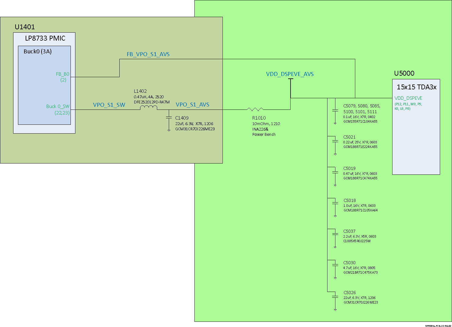
Figure 8-15 shows a PCB layout example and the resulting PI analysis results.
 Figure 8-15 vdd_dspeve Simplified SCH Diagram
 Table 8-8 DCap Scheme
| Vaule [uF] | Size | Qty | Capacitance [uF] |
|---|---|---|---|
| Cap Type: Automotive GCM series, X7R | |||
| 22 | 1206 | 1 | 22 |
| 4.7 | 805 | 1 | 4.7 |
| 2.2 | 603 | 1 | 2.2 |
| 1 | 603 | 1 | 1 |
| 0.47 | 603 | 1 | 0.47 |
| 0.22 | 603 | 1 | 0.22 |
| 0.1 | 402 | 6 | 0.6 |
| Totals | 12 | 31.19 | |
IR Drop: vdd_dspeve
![TDA3MV TDA3MA TDA3MD TDA3LX TDA3LA vdd_dspeve Voltage/IR Drop [All Layers] TDA3MV TDA3MA TDA3MD TDA3LX TDA3LA SPRS91v_PCB_CORE_06A.gif](/ods/images/JAJSE41G/SPRS91v_PCB_CORE_06A.gif) Figure 8-16 vdd_dspeve Voltage/IR Drop [All Layers]
Figure 8-16 vdd_dspeve Voltage/IR Drop [All Layers] Dynamic analysis of this PCB design for the CORE power domain determined the vdd_dspeve decoupling capacitor loop inductance and impedance vs frequency analysis shown below. As you can see, the loop inductance values ranged from 0.68 –1.79nH and were less than maximum 2.0nH recommended.
Table 8-9 Decoupling Design Detail Summary
| Cap Reference Description | Loop Inductacne at 50MHz [nH] | Footprint Types | PCB Side | Distance to Ball-Field [mils] | Value | Size |
|---|---|---|---|---|---|---|
| C5101 | 0.73 | 2vWEE | Bottom | 82 | 0.1 | 0402 |
| C5100 | 0.78 | 2vWEE | Bottom | 107 | 0.1 | 0402 |
| C5085 | 0.84 | 2vWEE | Bottom | 35 | 0.1 | 0402 |
| C5019 | 1.09 | 4vWE | Top | 631 | 0.47 | 0603 |
| C5111 | 1.09 | 4vWE | Bottom | 681 | 0.1 | 0402 |
| C5030 | 1.11 | 4vWE | Top | 738 | 4.7 | 0805 |
| C5037 | 1.11 | 4vWE | Top | 563 | 2.2 | 0603 |
| C5018 | 1.14 | 4vWE | Top | 681 | 1 | 0603 |
| C5021 | 1.17 | 4vWE | Top | 761 | 0.22 | 0603 |
| C5026 | 1.18 | 4vWE | Top | 792 | 22 | 1206 |
| C5079 | 1.32 | 4vWE | Bottom | 542 | 0.1 | 0402 |
| C5080 | 1.58 | 4vWE | Bottom | 602 | 0.1 | 0402 |
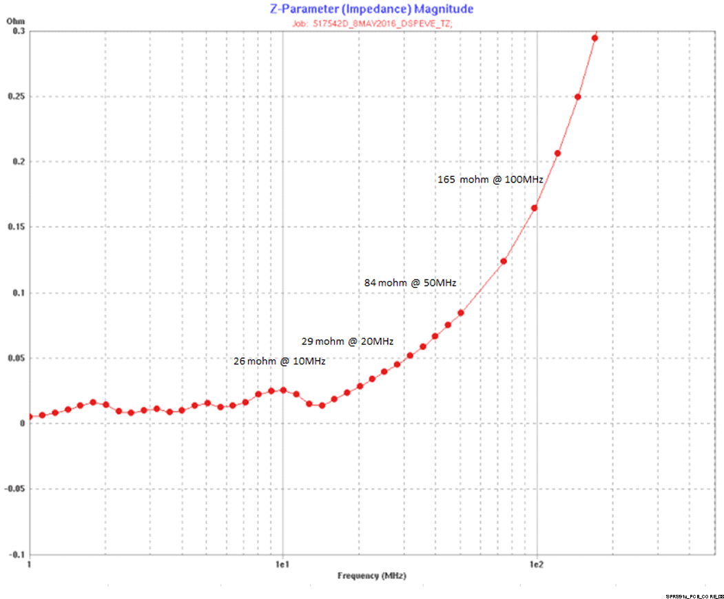
Figure 8-17 shows vdd_dspeve Impedance vs Frequency characteristics.
 Figure 8-17 vdd_dspeve Impedance vs Frequency