SPRSPB4A June   2024  – December 2024 TDA4APE-Q1 , TDA4VPE-Q1

PRODUCTION DATA  

  1.   1
  2. Features
  3. Applications
  4. Description
    1. 3.1 Functional Block Diagram
  5. Device Comparison
  6. Terminal Configuration and Functions
    1. 5.1 Pin Diagrams
    2. 5.2 Pin Attributes
      1.      10
      2.      11
    3. 5.3 Signal Descriptions
      1.      13
      2. 5.3.1  ADC
        1. 5.3.1.1 MCU Domain
          1.        16
          2.        17
          3.        18
      3. 5.3.2  CPSW2G
        1. 5.3.2.1 MAIN Domain
          1.        21
        2. 5.3.2.2 MCU Domain
          1.        23
      4. 5.3.3  CPTS
        1. 5.3.3.1 MAIN Domain
          1.        26
        2. 5.3.3.2 MCU Domain
          1.        28
      5. 5.3.4  CSI
        1. 5.3.4.1 MAIN Domain
          1.        31
          2.        32
          3.        33
      6. 5.3.5  DDRSS
        1. 5.3.5.1 MAIN Domain
          1.        36
          2.        37
      7. 5.3.6  Display Port
        1. 5.3.6.1 MAIN Domain
          1.        40
      8. 5.3.7  DMTIMER
        1. 5.3.7.1 MAIN Domain
          1.        43
        2. 5.3.7.2 MCU Domain
          1.        45
      9. 5.3.8  DSI
        1. 5.3.8.1 MAIN Domain
          1.        48
          2.        49
      10. 5.3.9  DSS
        1. 5.3.9.1 MAIN Domain
          1.        52
      11. 5.3.10 ECAP
        1. 5.3.10.1 MAIN Domain
          1.        55
          2.        56
          3.        57
      12. 5.3.11 EPWM
        1. 5.3.11.1 MAIN Domain
          1.        60
          2.        61
          3.        62
          4.        63
          5.        64
          6.        65
          7.        66
      13. 5.3.12 EQEP
        1. 5.3.12.1 MAIN Domain
          1.        69
          2.        70
          3.        71
      14. 5.3.13 GPIO
        1. 5.3.13.1 MAIN Domain
          1.        74
        2. 5.3.13.2 WKUP Domain
          1.        76
      15. 5.3.14 GPMC
        1. 5.3.14.1 MAIN Domain
          1.        79
      16. 5.3.15 HYPERBUS
        1. 5.3.15.1 MCU Domain
          1.        82
      17. 5.3.16 I2C
        1. 5.3.16.1 MAIN Domain
          1.        85
          2.        86
          3.        87
          4.        88
          5.        89
          6.        90
          7.        91
        2. 5.3.16.2 MCU Domain
          1.        93
          2.        94
        3. 5.3.16.3 WKUP Domain
          1.        96
      18. 5.3.17 I3C
        1. 5.3.17.1 MCU Domain
          1.        99
      19. 5.3.18 MCAN
        1. 5.3.18.1 MAIN Domain
          1.        102
          2.        103
          3.        104
          4.        105
          5.        106
          6.        107
          7.        108
          8.        109
          9.        110
          10.        111
          11.        112
          12.        113
          13.        114
          14.        115
          15.        116
          16.        117
          17.        118
          18.        119
        2. 5.3.18.2 MCU Domain
          1.        121
          2.        122
      20. 5.3.19 MCASP
        1. 5.3.19.1 MAIN Domain
          1.        125
          2.        126
          3.        127
          4.        128
          5.        129
      21. 5.3.20 MCSPI
        1. 5.3.20.1 MAIN Domain
          1.        132
          2.        133
          3.        134
          4.        135
          5.        136
          6.        137
          7.        138
        2. 5.3.20.2 MCU Domain
          1.        140
          2.        141
      22. 5.3.21 MDIO
        1. 5.3.21.1 MAIN Domain
          1.        144
          2.        145
        2. 5.3.21.2 MCU Domain
          1.        147
      23. 5.3.22 MMC
        1. 5.3.22.1 MAIN Domain
          1.        150
          2.        151
      24. 5.3.23 OSPI
        1. 5.3.23.1 MCU Domain
          1.        154
          2.        155
      25. 5.3.24 PCIE
        1. 5.3.24.1 MAIN Domain
          1.        158
      26. 5.3.25 SERDES
        1. 5.3.25.1 MAIN Domain
          1.        161
          2.        162
          3.        163
      27. 5.3.26 SGMII
        1. 5.3.26.1 MAIN Domain
          1.        166
      28. 5.3.27 UART
        1. 5.3.27.1 MAIN Domain
          1.        169
          2.        170
          3.        171
          4.        172
          5.        173
          6.        174
          7.        175
          8.        176
          9.        177
          10.        178
        2. 5.3.27.2 MCU Domain
          1.        180
        3. 5.3.27.3 WKUP Domain
          1.        182
      29. 5.3.28 UFS
        1. 5.3.28.1 MAIN Domain
          1.        185
      30. 5.3.29 USB
        1. 5.3.29.1 MAIN Domain
          1.        188
      31. 5.3.30 Emulation and Debug
        1. 5.3.30.1 MAIN Domain
          1.        191
          2.        192
      32. 5.3.31 System and Miscellaneous
        1. 5.3.31.1 Boot Mode Configuration
          1.        195
        2. 5.3.31.2 Clock
          1.        197
          2.        198
        3. 5.3.31.3 EFUSE
          1.        200
        4. 5.3.31.4 System
          1.        202
          2.        203
        5. 5.3.31.5 VMON
          1.        205
      33. 5.3.32 Power
        1.       207
    4. 5.4 Pin Connectivity Requirements
  7. Specifications
    1. 6.1  Absolute Maximum Ratings
    2. 6.2  ESD Ratings
    3. 6.3  Power-On-Hour (POH) Limits
    4. 6.4  Recommended Operating Conditions
    5. 6.5  Operating Performance Points
    6. 6.6  Electrical Characteristics
      1. 6.6.1  I2C, Open-Drain, Fail-Safe (I2C OD FS) Electrical Characteristics
      2. 6.6.2  Fail-Safe Reset (FS Reset) Electrical Characteristics
      3. 6.6.3  HFOSC/LFOSC Electrical Characteristics
      4. 6.6.4  eMMCPHY Electrical Characteristics
      5. 6.6.5  SDIO Electrical Characteristics
      6. 6.6.6  CSI2/DSI D-PHY Electrical Characteristics
      7. 6.6.7  ADC12B Electrical Characteristics
      8. 6.6.8  LVCMOS Electrical Characteristics
      9. 6.6.9  USB2PHY Electrical Characteristics
      10. 6.6.10 SerDes 2-L-PHY/4-L-PHY Electrical Characteristics
      11. 6.6.11 UFS M-PHY Electrical Characteristics
      12. 6.6.12 eDP/DP AUX-PHY Electrical Characteristics
      13. 6.6.13 DDR0 Electrical Characteristics
    7. 6.7  VPP Specifications for One-Time Programmable (OTP) eFuses
      1. 6.7.1 Recommended Operating Conditions for OTP eFuse Programming
      2. 6.7.2 Hardware Requirements
      3. 6.7.3 Programming Sequence
      4. 6.7.4 Impact to Your Hardware Warranty
    8. 6.8  Thermal Resistance Characteristics
      1. 6.8.1 Thermal Resistance Characteristics for AND Package
    9. 6.9  Temperature Sensor Characteristics
    10. 6.10 Timing and Switching Characteristics
      1. 6.10.1 Timing Parameters and Information
      2. 6.10.2 Power Supply Sequencing
        1. 6.10.2.1 Power Supply Slew Rate Requirement
        2. 6.10.2.2 Combined MCU and Main Domains Power- Up Sequencing
        3. 6.10.2.3 Combined MCU and Main Domains Power- Down Sequencing
        4. 6.10.2.4 Isolated MCU and Main Domains Power- Up Sequencing
        5. 6.10.2.5 Isolated MCU and Main Domains Power- Down Sequencing
        6. 6.10.2.6 Independent MCU and Main Domains, Entry and Exit of MCU Only Sequencing
        7. 6.10.2.7 Independent MCU and Main Domains, Entry and Exit of DDR Retention State
        8. 6.10.2.8 Independent MCU and Main Domains, Entry and Exit of GPIO Retention Sequencing
      3. 6.10.3 System Timing
        1. 6.10.3.1 Reset Timing
        2. 6.10.3.2 Safety Signal Timing
        3. 6.10.3.3 Clock Timing
      4. 6.10.4 Clock Specifications
        1. 6.10.4.1 Input and Output Clocks / Oscillators
          1. 6.10.4.1.1 WKUP_OSC0 Internal Oscillator Clock Source
            1. 6.10.4.1.1.1 Load Capacitance
            2. 6.10.4.1.1.2 Shunt Capacitance
          2. 6.10.4.1.2 WKUP_OSC0 LVCMOS Digital Clock Source
          3. 6.10.4.1.3 Auxiliary OSC1 Internal Oscillator Clock Source
            1. 6.10.4.1.3.1 Load Capacitance
            2. 6.10.4.1.3.2 Shunt Capacitance
          4. 6.10.4.1.4 Auxiliary OSC1 LVCMOS Digital Clock Source
          5. 6.10.4.1.5 Auxiliary OSC1 Not Used
        2. 6.10.4.2 Output Clocks
        3. 6.10.4.3 PLLs
        4. 6.10.4.4 Module and Peripheral Clocks Frequencies
      5. 6.10.5 Peripherals
        1. 6.10.5.1  ATL
          1. 6.10.5.1.1 ATL_PCLK Timing Requirements
          2. 6.10.5.1.2 ATL_AWS[x] Timing Requirements
          3. 6.10.5.1.3 ATL_BWS[x] Timing Requirements
          4. 6.10.5.1.4 ATCLK[x] Switching Characteristics
        2. 6.10.5.2  CPSW2G
          1. 6.10.5.2.1 CPSW2G MDIO Interface Timings
          2. 6.10.5.2.2 CPSW2G RMII Timings
            1. 6.10.5.2.2.1 CPSW2G RMII[x]_REF_CLK Timing Requirements – RMII Mode
            2. 6.10.5.2.2.2 CPSW2G RMII[x]_RXD[1:0], RMII[x]_CRS_DV, and RMII[x]_RX_ER Timing Requirements – RMII Mode
            3. 6.10.5.2.2.3 CPSW2G RMII[x]_TXD[1:0], and RMII[x]_TX_EN Switching Characteristics – RMII Mode
          3. 6.10.5.2.3 CPSW2G RGMII Timings
            1. 6.10.5.2.3.1 RGMII[x]_RXC Timing Requirements – RGMII Mode
            2. 6.10.5.2.3.2 CPSW2G Timing Requirements for RGMII[x]_RD[3:0], and RGMII[x]_RCTL – RGMII Mode
            3. 6.10.5.2.3.3 CPSW2G RGMII[x]_TXC Switching Characteristics – RGMII Mode
            4. 6.10.5.2.3.4 RGMII[x]_TD[3:0], and RGMII[x]_TX_CTL Switching Characteristics – RGMII Mode
        3. 6.10.5.3  CSI-2
        4. 6.10.5.4  DDRSS
        5. 6.10.5.5  DSS
        6. 6.10.5.6  eCAP
          1. 6.10.5.6.1 Timing Requirements for eCAP
          2. 6.10.5.6.2 Switching Characteristics for eCAP
        7. 6.10.5.7  EPWM
          1. 6.10.5.7.1 Timing Requirements for eHRPWM
          2. 6.10.5.7.2 Switching Characteristics for eHRPWM
        8. 6.10.5.8  eQEP
          1. 6.10.5.8.1 Timing Requirements for eQEP
          2. 6.10.5.8.2 Switching Characteristics for eQEP
        9. 6.10.5.9  GPIO
          1. 6.10.5.9.1 GPIO Timing Requirements
          2. 6.10.5.9.2 GPIO Switching Characteristics
        10. 6.10.5.10 GPMC
          1. 6.10.5.10.1 GPMC and NOR Flash — Synchronous Mode
            1. 6.10.5.10.1.1 GPMC and NOR Flash Timing Requirements — Synchronous Mode
            2. 6.10.5.10.1.2 GPMC and NOR Flash Switching Characteristics – Synchronous Mode
          2. 6.10.5.10.2 GPMC and NOR Flash — Asynchronous Mode
            1. 6.10.5.10.2.1 GPMC and NOR Flash Timing Requirements – Asynchronous Mode
            2. 6.10.5.10.2.2 GPMC and NOR Flash Switching Characteristics – Asynchronous Mode
          3. 6.10.5.10.3 GPMC and NAND Flash — Asynchronous Mode
            1. 6.10.5.10.3.1 GPMC and NAND Flash Timing Requirements – Asynchronous Mode
            2. 6.10.5.10.3.2 GPMC and NAND Flash Switching Characteristics – Asynchronous Mode
          4. 6.10.5.10.4 GPMC0 IOSET
        11. 6.10.5.11 HyperBus
          1. 6.10.5.11.1 Timing Requirements for HyperBus
          2. 6.10.5.11.2 HyperBus 166 MHz Switching Characteristics
          3. 6.10.5.11.3 HyperBus 100 MHz Switching Characteristics
        12. 6.10.5.12 I2C
        13. 6.10.5.13 I3C
        14. 6.10.5.14 MCAN
        15. 6.10.5.15 MCASP
        16. 6.10.5.16 MCSPI
          1. 6.10.5.16.1 MCSPI — Controller Mode
          2. 6.10.5.16.2 MCSPI — Peripheral Mode
        17. 6.10.5.17 MMCSD
          1. 6.10.5.17.1 MMC0 - eMMC Interface
            1. 6.10.5.17.1.1 Legacy SDR Mode
            2. 6.10.5.17.1.2 High Speed SDR Mode
            3. 6.10.5.17.1.3 High Speed DDR Mode
            4. 6.10.5.17.1.4 HS200 Mode
            5. 6.10.5.17.1.5 HS400 Mode
          2. 6.10.5.17.2 MMC1/2 - SD/SDIO Interface
            1. 6.10.5.17.2.1 Default Speed Mode
            2. 6.10.5.17.2.2 High Speed Mode
            3. 6.10.5.17.2.3 UHS–I SDR12 Mode
            4. 6.10.5.17.2.4 UHS–I SDR25 Mode
            5. 6.10.5.17.2.5 UHS–I SDR50 Mode
            6. 6.10.5.17.2.6 UHS–I DDR50 Mode
            7. 6.10.5.17.2.7 UHS–I SDR104 Mode
        18. 6.10.5.18 CPTS
          1. 6.10.5.18.1 CPTS Timing Requirements
          2. 6.10.5.18.2 CPTS Switching Characteristics
        19. 6.10.5.19 OSPI
          1. 6.10.5.19.1 OSPI0/1 PHY Mode
            1. 6.10.5.19.1.1 OSPI0/1 With PHY Data Training
            2. 6.10.5.19.1.2 OSPI Without Data Training
              1. 6.10.5.19.1.2.1 OSPI Timing Requirements – SDR Mode
              2. 6.10.5.19.1.2.2 OSPI Switching Characteristics – SDR Mode
              3. 6.10.5.19.1.2.3 OSPI Timing Requirements – DDR Mode
              4. 6.10.5.19.1.2.4 OSPI Switching Characteristics – PHY DDR Mode
          2. 6.10.5.19.2 OSPI0/1 Tap Mode
            1. 6.10.5.19.2.1 OSPI0 Tap SDR Timing
            2. 6.10.5.19.2.2 OSPI0 Tap DDR Timing
        20. 6.10.5.20 OLDI
          1. 6.10.5.20.1 OLDI Switching Characteristics
        21. 6.10.5.21 PCIE
        22. 6.10.5.22 Timers
          1. 6.10.5.22.1 Timing Requirements for Timers
          2. 6.10.5.22.2 Switching Characteristics for Timers
        23. 6.10.5.23 UART
          1. 6.10.5.23.1 Timing Requirements for UART
          2. 6.10.5.23.2 UART Switching Characteristics
        24. 6.10.5.24 USB
      6. 6.10.6 Emulation and Debug
        1. 6.10.6.1 Trace
        2. 6.10.6.2 JTAG
          1. 6.10.6.2.1 JTAG Electrical Data and Timing
            1. 6.10.6.2.1.1 JTAG Timing Requirements
            2. 6.10.6.2.1.2 JTAG Switching Characteristics
  8. Applications, Implementation, and Layout
    1. 7.1 Device Connection and Layout Fundamentals
      1. 7.1.1 Power Supply Decoupling and Bulk Capacitors
        1. 7.1.1.1 Power Distribution Network Implementation Guidance
      2. 7.1.2 External Oscillator
      3. 7.1.3 JTAG and EMU
      4. 7.1.4 Reset
      5. 7.1.5 Unused Pins
      6. 7.1.6 Hardware Design Guide for JacintoTM 7 Devices
    2. 7.2 Peripheral- and Interface-Specific Design Information
      1. 7.2.1 LPDDR4 Board Design and Layout Guidelines
      2. 7.2.2 OSPI and QSPI Board Design and Layout Guidelines
        1. 7.2.2.1 No Loopback and Internal Pad Loopback
        2. 7.2.2.2 External Board Loopback
        3. 7.2.2.3 DQS (only available in Octal Flash devices)
      3. 7.2.3 USB VBUS Design Guidelines
      4. 7.2.4 System Power Supply Monitor Design Guidelines using VMON/POK
      5. 7.2.5 High Speed Differential Signal Routing Guidance
      6. 7.2.6 Thermal Solution Guidance
  9. Device and Documentation Support
    1. 8.1 Device Nomenclature
      1. 8.1.1 Standard Package Symbolization
      2. 8.1.2 Device Naming Convention
    2. 8.2 Tools and Software
    3. 8.3 Support Resources
    4. 8.4 Trademarks
    5. 8.5 Electrostatic Discharge Caution
    6. 8.6 Glossary
  10. Revision History
  11. 10Mechanical, Packaging, and Orderable Information
    1. 10.1 Packaging Information

パッケージ・オプション

デバイスごとのパッケージ図は、PDF版データシートをご参照ください。

メカニカル・データ(パッケージ|ピン)
  • AND|1063
サーマルパッド・メカニカル・データ
発注情報

OSPI0/1 With PHY Data Training

Read and write data valid windows will shift due to variation in process, voltage, temperature, and operating frequency. A data training method may be implemented to dynamically configure optimal read and write timing. Implementing data training enables proper operation across temperature with a specific process, voltage, and frequency operating condition, while achieving a higher operating frequency.

Data transmit and receive timing parameters are not defined for the data training use case since they are dynamically adjusted based on the operating condition.

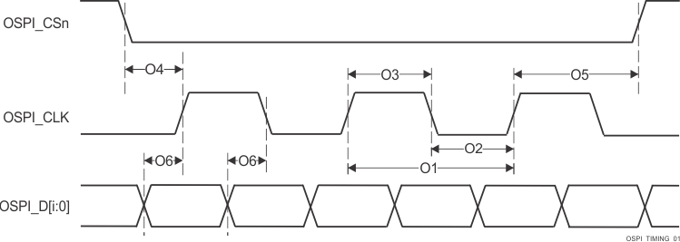
Table 6-83 defines DLL delays required for OSPI0/1 with Data Training. Table 6-84, Figure 6-99, Figure 6-100, Table 6-85, Figure 6-101, and Figure 6-102 present timing requirements and switching characteristics for OSPI0/1 with Data Training.

Table 6-83 OSPI0/1 DLL Delay Mapping for PHY Data Training
MODE OSPI_PHY_CONFIGURATION_REG BIT FIELD DELAY VALUE
Transmit
All modes PHY_CONFIG_TX_DLL_DELAY_FLD (1)
Receive
All modes PHY_CONFIG_RX_DLL_DELAY_FLD (2)
Transmit DLL delay value determined by training software
Receive DLL delay value determined by training software
Table 6-84 OSPI0 Timing Requirements – PHY Data Training see Figure 6-99, and Figure 6-100
NO. MODE MIN MAX UNIT
O15 tsu(D-LBCLK) Setup time, OSPI0_D[7:0] valid before active OSPI0_DQS edge DDR with DQS (1) ns
O16 th(LBCLK-D) Hold time, OSPI0_D[7:0] valid after active OSPI0_DQS edge DDR with DQS (1) ns
O21 tsu(D-LBCLK) Setup time, OSPI0_D[7:0] valid before active OSPI0_DQS edge SDR with Internal PHY Loopback (1) ns
O22 th(LBCLK-D) Hold time, OSPI0_D[7:0] valid after active OSPI0_DQS edge SDR with Internal PHY Loopback (1) ns
tDVW Data valid window (O15 + O16) 1.8V, DDR with DQS 1.4 ns
Data valid window (O21 + O22) 1.8V, SDR with Internal PHY Loopback 1.7 ns
Minimum setup and hold time requirements for OSPI0/1_D[7:0] inputs are not defined when Data Training is used to find the optimum data valid window. The tDVW parameter defines the minimum data invalid window required. This parameter is provided in lieu of minimum setup and minimum hold times, where it must be used to check compatibility with the data valid window provided by an attached device.
TDA4VPE-Q1 TDA4APE-Q1 OSPI0/1 Timing Requirements – PHY Data Training, DDR with DQS Figure 6-99 OSPI0/1 Timing Requirements – PHY Data Training, DDR with DQS
TDA4VPE-Q1 TDA4APE-Q1 OSPI0/1 Timing Requirements – PHY Data Training, SDR with Internal PHY Loopback Figure 6-100 OSPI0/1 Timing Requirements – PHY Data Training, SDR with Internal PHY Loopback
Table 6-85 OSPI/1 Switching Characteristics – PHY Data Training See Figure 6-101 and Figure 6-102
NO. PARAMETER MODE MIN MAX UNIT
O1 tc(CLK) Cycle time, OSPI0/1_CLK 1.8V, DDR 6.0 6.0 ns
O7 1.8V, SDR 6.0 6.0 ns
O2 tw(CLKL) Pulse duration, OSPI0/1_CLK low DDR ((0.475P(1)) - 0.3) ns
O8 SDR
O3 tw(CLKH) Pulse duration, OSPI0/1_CLK high DDR ((0.475P(1)) - 0.3) ns
O9 SDR
O4 td(CSn-CLK) Delay time, OSPI0/1_CSn[3:0] active edge to OSPI0/1_CLK rising edge DDR ((0.475P(1)) + (0.975M(2)R(4)) + (0.028TD(5)) - 1) ((0.525P(1)) + (1.025M(2)R(4)) + (0.055TD(5)) + 1) ns
O10 SDR
O5 td(CLK-CSn) Delay time, OSPI0/1_CLK rising edge to OSPI0/1_CSn[3:0] inactive edge DDR ((0.475P(1)) + (0.975N(3)R(4)) - (0.055TD(5)) - 1) ((0.525P(1)) + (1.025N(3)R(4)) - (0.028TD(5)) + 1) ns
O11 SDR
O6 td(CLK-D) Delay time, OSPI0/1_CLK active edge to OSPI0/1_D[7:0] transition DDR (6) (6) ns
O12 SDR
tDIVW Data invalid window (O6 Max - Min) DDR 1 ns
Data invalid window (O12 Max - Min) SDR
P = SCLK cycle time in ns = OSPI0_CLK cycle time in ns
M = OSPI_DEV_DELAY_REG[D_INIT_FLD]
N = OSPI_DEV_DELAY_REG[D_AFTER_FLD]
R = reference clock cycle time in ns
TD = PHY_CONFIG_TX_DLL_DELAY_FLD
Minimum and maximum delay times for OSPI0_D[7:0] outputs are not defined when Data Training is used to find the optimum data valid window. The tDIVW parameter defines the maximum data invalid window. This parameter is provided in lieu of minimum and maximum delay times, where it must be used to check compatibility with the data valid window requirements of an attached device.
TDA4VPE-Q1 TDA4APE-Q1 OSPI0/1 Switching Characteristics – PHY DDR Data Training Figure 6-101 OSPI0/1 Switching Characteristics – PHY DDR Data Training
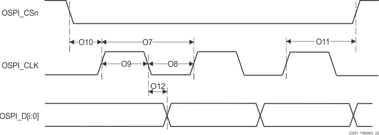
TDA4VPE-Q1 TDA4APE-Q1 OSPI0/1 Switching Characteristics – PHY SDR Data Training Figure 6-102 OSPI0/1 Switching Characteristics – PHY SDR Data Training