JAJSIF7K September 2021 – April 2024 TDA4VM , TDA4VM-Q1
PRODUCTION DATA
- 1
- 1 特長
- 2 アプリケーション
- 3 概要
- 4 Device Comparison
-
5 Terminal Configuration and Functions
- 5.1 Pin Diagram
- 5.2 Pin Attributes
- 5.3
Signal Descriptions
- 5.3.1 ADC
- 5.3.2 DDRSS
- 5.3.3 GPIO
- 5.3.4 I2C
- 5.3.5 I3C
- 5.3.6 MCAN
- 5.3.7 MCSPI
- 5.3.8 UART
- 5.3.9 MDIO
- 5.3.10 CPSW2G
- 5.3.11 CPSW9G
- 5.3.12 ECAP
- 5.3.13 EQEP
- 5.3.14 EHRPWM
- 5.3.15 USB
- 5.3.16 SERDES
- 5.3.17 OSPI
- 5.3.18 Hyperbus
- 5.3.19 GPMC
- 5.3.20 MMC
- 5.3.21 CPTS
- 5.3.22 UFS
- 5.3.23 PRU_ICSSG [Currently Not Supported]
- 5.3.24 MCASP
- 5.3.25 DSS
- 5.3.26 DP
- 5.3.27 Camera Streaming Interface Receiver (CSI_RX_IF) Subsystem
- 5.3.28 DSI_TX
- 5.3.29 VPFE
- 5.3.30 DMTIMER
- 5.3.31 Emulation and Debug
- 5.3.32 System and Miscellaneous
- 5.3.33 Power Supply
- 5.4 Pin Multiplexing
- 5.5 Pin Connectivity Requirements
-
6 Specifications
- 6.1 Absolute Maximum Ratings
- 6.2 ESD Ratings
- 6.3 Power-On-Hour (POH) Limits
- 6.4 Recommended Operating Conditions
- 6.5 Operating Performance Points
- 6.6 Electrical Characteristics
- 6.7 VPP Specifications for One-Time Programmable (OTP) eFuses
- 6.8 Thermal Resistance Characteristics
- 6.9
Timing and Switching Characteristics
- 6.9.1 Timing Parameters and Information
- 6.9.2
Power Supply Sequencing
- 6.9.2.1 Power Supply Slew Rate Requirement
- 6.9.2.2 Combined MCU and Main Domains Power-Up Sequencing
- 6.9.2.3 Combined MCU and Main Domains Power- Down Sequencing
- 6.9.2.4 Isolated MCU and Main Domains Power- Up Sequencing
- 6.9.2.5 Isolated MCU and Main Domains, Primary Power- Down Sequencing
- 6.9.2.6 Entry and Exit of MCU Only State
- 6.9.2.7 Entry and Exit of DDR Retention State
- 6.9.3 System Timing
- 6.9.4
Clock Specifications
- 6.9.4.1
Input and Output Clocks / Oscillators
- 6.9.4.1.1 WKUP_OSC0 Internal Oscillator Clock Source
- 6.9.4.1.2 WKUP_OSC0 LVCMOS Digital Clock Source
- 6.9.4.1.3 Auxiliary OSC1 Internal Oscillator Clock Source
- 6.9.4.1.4 Auxiliary OSC1 LVCMOS Digital Clock Source
- 6.9.4.1.5 Auxiliary OSC1 Not Used
- 6.9.4.1.6 WKUP_LFOSC0 Internal Oscillator Clock Source
- 6.9.4.1.7 WKUP_LFOSC0 Not Used
- 6.9.4.2 Output Clocks
- 6.9.4.3 PLLs
- 6.9.4.4 Module and Peripheral Clocks Frequencies
- 6.9.4.1
Input and Output Clocks / Oscillators
- 6.9.5
Peripherals
- 6.9.5.1 ATL
- 6.9.5.2 VPFE
- 6.9.5.3
CPSW2G
- 6.9.5.3.1 CPSW2G MDIO Interface Timings
- 6.9.5.3.2 CPSW2G RMII Timings
- 6.9.5.3.3
CPSW2G RGMII Timings
- 6.9.5.3.3.1 RGMII[x]_RXC Timing Requirements – RGMII Mode
- 6.9.5.3.3.2 CPSW2G Timing Requirements for RGMII[x]_RD[3:0], and RGMII[x]_RCTL – RGMII Mode
- 6.9.5.3.3.3 CPSW2G RGMII[x]_TXC Switching Characteristics – RGMII Mode
- 6.9.5.3.3.4 RGMII[x]_TD[3:0], and RGMII[x]_TX_CTL Switching Characteristics – RGMII Mode
- 6.9.5.4 CPSW9G
- 6.9.5.5 CSI-2
- 6.9.5.6 DDRSS
- 6.9.5.7 DSS
- 6.9.5.8 eCAP
- 6.9.5.9 EPWM
- 6.9.5.10 eQEP
- 6.9.5.11 GPIO
- 6.9.5.12 GPMC
- 6.9.5.13 HyperBus
- 6.9.5.14 I2C
- 6.9.5.15 I3C
- 6.9.5.16 MCAN
- 6.9.5.17 MCASP
- 6.9.5.18 MCSPI
- 6.9.5.19 MMCSD
- 6.9.5.20 CPTS
- 6.9.5.21 OSPI
- 6.9.5.22 PCIE
- 6.9.5.23 Timers
- 6.9.5.24 UART
- 6.9.5.25 USB
- 6.9.6 Emulation and Debug
-
7 Detailed Description
- 7.1 Overview
- 7.2 Processor Subsystems
- 7.3 Accelerators and Coprocessors
- 7.4
Other Subsystems
- 7.4.1 MSMC
- 7.4.2 NAVSS
- 7.4.3 PDMA Controller
- 7.4.4 Power Supply
- 7.4.5
Peripherals
- 7.4.5.1 ADC
- 7.4.5.2 ATL
- 7.4.5.3 CSI
- 7.4.5.4 CPSW2G
- 7.4.5.5 CPSW9G
- 7.4.5.6 DCC
- 7.4.5.7 DDRSS
- 7.4.5.8 DSS
- 7.4.5.9 VPFE
- 7.4.5.10 eCAP
- 7.4.5.11 EPWM
- 7.4.5.12 ELM
- 7.4.5.13 ESM
- 7.4.5.14 eQEP
- 7.4.5.15 GPIO
- 7.4.5.16 GPMC
- 7.4.5.17 Hyperbus
- 7.4.5.18 I2C
- 7.4.5.19 I3C
- 7.4.5.20 MCAN
- 7.4.5.21 MCASP
- 7.4.5.22 MCRC Controller
- 7.4.5.23 MCSPI
- 7.4.5.24 MMC/SD
- 7.4.5.25 OSPI
- 7.4.5.26 PCIE
- 7.4.5.27 SerDes
- 7.4.5.28 WWDT
- 7.4.5.29 Timers
- 7.4.5.30 UART
- 7.4.5.31 USB
- 7.4.5.32 UFS
-
8 Applications and
Implementation
- 8.1 Power Supply Mapping
- 8.2 Device Connection and Layout Fundamentals
- 8.3
Peripheral- and Interface-Specific Design Information
- 8.3.1 LPDDR4 Board Design and Layout Guidelines
- 8.3.2 OSPI and QSPI Board Design and Layout Guidelines
- 8.3.3 SERDES REFCLK Design Guidelines
- 8.3.4 USB VBUS Design Guidelines
- 8.3.5 System Power Supply Monitor Design Guidelines
- 8.3.6 High Speed Differential Signal Routing Guidance
- 8.3.7 Thermal Solution Guidance
- 9 Device and Documentation Support
- 10Revision History
- 11Mechanical, Packaging, and Orderable Information
パッケージ・オプション
デバイスごとのパッケージ図は、PDF版データシートをご参照ください。
メカニカル・データ(パッケージ|ピン)
- ALF|827
サーマルパッド・メカニカル・データ
発注情報
6.9.4.1.6 WKUP_LFOSC0 Internal Oscillator Clock Source
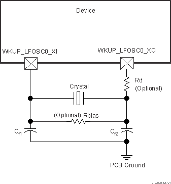
Figure 6-34 shows the recommended crystal circuit. It is recommended that preproduction printed-circuit board (PCB) designs include the two optional resistors Rbias and Rd in case they are required for proper oscillator operation when combined with production crystal circuit components. In most cases, Rbias is not required and Rd is a 0-Ω resistor. These resistors may be removed from production PCB designs after evaluating oscillator performance with production crystal circuit components installed on preproduction PCBs.
 Figure 6-34 WKUP_LFOSC0 Crystal Implementation
Table 6-33 presents LFXOSC modes of operation.
| MODE | BP_C | PD_C | XI | XO | CLK_OUT | DESCRIPTION |
|---|---|---|---|---|---|---|
| ACTIVE | 0 | 0 | XTAL | XTAL | CLK_OUT | Active oscillator mode providing 32kHz |
| PWRDN | 0 | 1 | X | PD | LOW | Output will be pulled down to LOW. PAD to be tri-stated. Active mode disabled |
| BYPASS | 1 | 0 | CLK | PD | CLK | XI is driven by external clock source. XO is pulled down to LOW. Due to ESD diode to supply, XI should not be driven unless oscillator supply is present. |
User should set CTRLMMR_WKUP_LFXOSC_TRIM[18:16] i_mult = 3b’001 for CL in the range 6pf to 9.5pf. CTRLMMR_WKUP_LFXOSC_TRIM [18:16] i_mult = 3b’010 for CL in the range 8.5pf to 12pf. Default setting is 3b’010.
The load capacitors, Cf1 and Cf2 in Figure 6-35, should be chosen such that the below equation is satisfied. CL in the equation is the load specified by the crystal manufacturer. All discrete components used to implement the oscillator circuit should be placed as close as possible to the associated oscillator WKUP_LFOSC0_XI, WKUP_LFOSC0_XO, and VSS pins.
 Figure 6-35 Load
Capacitance Equation
Figure 6-35 Load
Capacitance EquationThe crystal must be in the fundamental mode of operation and parallel resonant. Table 6-34 summarizes the required electrical constraints.
| NAME | DESCRIPTION | MIN | TYP | MAX | UNIT | |||
|---|---|---|---|---|---|---|---|---|
| fp | Parallel resonance crystal frequency | 32768 | Hz | |||||
| Cf1 | Cf1 load capacitance for crystal parallel resonance with Cf1 = Cf2 | 12 | 24 | pF | ||||
| Cf2 | Cf2 load capacitance for crystal parallel resonance with Cf1 = Cf2 | 12 | 24 | pF | ||||
| Cshunt | Shunt capacitance | ESRxtal – 40 Ω | 4 | pF | ||||
| ESRxtal – 60 Ω | 3 | pF | ||||||
| ESRxtal – 80 Ω | 2 | pF | ||||||
| ESRxtal – 100 Ω | 1 | pF | ||||||
| ESR | Crystal effective series resistance | 100 | kΩ | |||||
When selecting a crystal, the system design must consider the temperature and aging characteristics of a based on the worst case environment and expected life expectancy of the system.
Table 6-35 details the switching characteristics of the oscillator and the requirements of the input clock.
| NAME | DESCRIPTION | MIN | TYP | MAX | UNIT |
|---|---|---|---|---|---|
| fxtal | Oscillation frequency | 32768 | Hz | ||
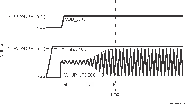
| tsX | Start-up time | 96.5 | ms |
 Figure 6-36 WKUP_LFOSC0 Start-up Time