SNAS670 July 2015 TDC1011-Q1
PRODUCTION DATA.
- 1 Features
- 2 Applications
- 3 Description
- 4 Revision History
- 5 Pin Configuration and Functions
- 6 Specifications
- 7 Parameter Measurement Information
-
8 Detailed Description
- 8.1 Overview
- 8.2 Functional Block Diagram
- 8.3 Feature Description
- 8.4 Device Function Description
- 8.5 Programming
- 8.6
Register Maps
- 8.6.1
TDC1011 Registers
- 8.6.1.1 CONFIG_0 Register (address = 0h) [reset = 45h]
- 8.6.1.2 CONFIG_1 Register (address = 1h) [reset = 40h]
- 8.6.1.3 CONFIG_2 Register (address = 2h) [reset = 0h]
- 8.6.1.4 CONFIG_3 Register (address 3h) [reset = 3h]
- 8.6.1.5 CONFIG_4 Register (address = 4h) [reset = 1Fh]
- 8.6.1.6 TOF_1 Register (address = 5h) [reset = 0h]
- 8.6.1.7 TOF_0 Register (address = 6h) [reset = 0h]
- 8.6.1.8 ERROR_FLAGS Register (address = 7h) [reset = 0h]
- 8.6.1.9 TIMEOUT Register (address = 8h) [reset = 19h]
- 8.6.1.10 CLOCK_RATE Register (address = 9h) [reset = 0h]
- 8.6.1
TDC1011 Registers
- 9 Application and Implementation
- 10Power Supply Recommendations
- 11Layout
- 12Device and Documentation Support
- 13Mechanical, Packaging, and Orderable Information
8 Detailed Description
8.1 Overview
The main functional blocks of TDC1011 are the Transmit (TX) and the Receive (RX) Channels. The transmitter supports flexible settings for driving various ultrasonic transducers, and the receiver provides configurable blocks with a wide range of settings for signal conditioning in various applications. The receive signal chain consists of an LNA (Low Noise Amplifier), a PGA (Programmable Gain Amplifier), and two auto-zeroed comparators for echo qualification and STOP pulse generation.
A measurement cycle is initiated with a trigger signal on the TRIGGER pin of the device. After a trigger signal is asserted, an output pulse is generated on the START pin. This signal is used as the time reference to begin a TOF measurement. The transmitter generates programmable TX pulses, synchronous to the rising edge of the START pulse, to drive an ultrasonic transducer and generate an ultrasonic wave that is shot through an acoustic medium. The receiver detects the ultrasound wave that traveled through the medium and generates STOP signals. Whether the ultrasound wave is received directly or from a reflection will depend on the system configuration. The STOP signals are used by an external Time-to-Digital Converter (TDC), which functions as a very accurate stopwatch. The system must include a TDC to measure the TOF based on the interval between the START and STOP pulses. In some applications with medium-range accuracy requirements (ns range), a microcontroller can be used to measure the TOF duration. In applications with high-range accuracy requirements (ps range), TI recommends using the TDC7200 time-to-digital converter to measure the TOF duration.
In each application, the TDC1011 has to be configured by a serial interface (SPI) for the various application-specific parameters that are explained in the following sections.
8.2 Functional Block Diagram
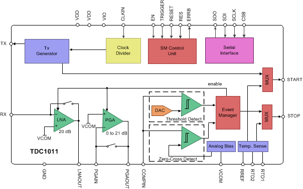
8.3 Feature Description
8.3.1 Transmitter Signal Path
The Transmitter (TX) path consists of a Clock Divider block and a TX Generator block. The clock divider allows the TDC1011 to divide the clock source that is connected to the CLKIN pin down to the resonant frequency (ƒR) of the transducer used. The clock divider allows division factors in powers of 2. The division factor of the clock divider can be programmed with the TX_FREQ_DIV field in the CONFIG_0 register.
The TX Generator block can drive a transducer with a programmable number of TX pulses. The frequency of these pulses is defined as ƒCLKIN/(2TX_FREQ_DIV+1), and should match the ƒR of the transducer. The number of pulses is configured by programming the NUM_TX field in the CONFIG_0 register.
For example, for ƒCLKIN = 8 MHz and TX_FREQ_DIV = 2h (divide by 8), the divided clock frequency is 1 MHz.
In addition to the programmable number of pulses, the TX Generator also provides options to introduce a 180⁰ pulse shift at pulse position n or damping the last TX pulse. In some situations, damping can reduce the ringing of the transducer for very short TOF measurements. These features are further described in the TRANSMIT Operation section of the datasheet.
8.3.2 Receiver Signal Path
The RX signal path consists of an LNA, PGA, and a pair of comparators. The LNA and PGA provide the required amplification of the receive signal. The amplified receive signal is fed into a set of comparators which generate pulses on the STOP pin based on the programmed threshold levels. The block diagram for the receiver path can be seen in Figure 15.
If the 20-dB to 41-dB of gain provided by the TDC1011 is insufficient, additional gain can be added prior to the COMPIN pin. Likewise, with a strong received signal, if the gain from the LNA or PGA is not needed, they can be bypassed and the transducer signal can be directly connected to the COMPIN pin.
A band-pass filter centered on the transducer’s response can be used between each stage of the receiver path to reduce the noise; note that the inputs of the LNA, PGA, and comparators should be biased to the VCOM pin’s potential. The comparators connected to the COMPIN pin are used for echo qualification and generation of STOP pulses that correspond to the zero-crossings of the echo signal. The STOP pulses are used with a START pulse to calculate the TOF of the echo in the medium.
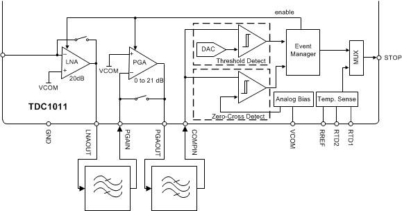 Figure 15. TDC1011 Receiver Path
8.3.3 Low Noise Amplifier (LNA)
The LNA in the TDC1011’s front-end limits the input-referred noise and ensures timing accuracy for the generated STOP pulses. The LNA is an inverting amplifier designed for a closed-loop gain of 20 dB with the aid of an external input capacitor or resistor, and it can be programmed for two feedback configurations. The band-pass configuration, referred to as capacitive feedback mode, must be combined with an input capacitor. The low-pass configuration, referred to as resistive feedback mode, must be combined with an input resistor. The recommended values for the input components are 300 pF and 900 Ω respectively.
The LNA can be configured in capacitive feedback mode for transducers with resonant frequencies in the order of a couple of MHz. This is done by clearing the LNA_FB bit in the TOF_1 register to 0. As shown in Figure 16, the external capacitor, CIN, should be placed between the transducer and the input pin. This provides an in-band gain of CIN/CF, where CF is the on-chip 30-pF feedback capacitor. Provided that CIN = 300 pF, the in-band gain of the LNA circuit is:

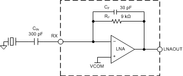 Figure 16. LNA Capacitive Feedback Configuration
The capacitive feedback configuration of the LNA has a band-pass frequency response. The high-pass corner frequency is set by the internal feedback components RF (9 kΩ) and CF (30 pF), and is approximately 590 kHz. The in-band gain is set by the capacitor ratio and the LNA’s 50-MHz gain-bandwidth product sets the low-pass corner of the frequency response. For example, an in-band gain of 10 results in a bandpass response between 590 kHz and 5 MHz.
The LNA can be configured in resistive feedback mode for transducers with resonant frequencies in the order of a couple of hundreds of kHz. This is done by setting the LNA_FB bit in the TOF_1 register to 1. In this configuration, the internal feedback capacitor CF is disconnected (see Figure 17), and the DC gain of the LNA circuit is determined by the ratio between the internal feedback resistor RF (9 kΩ) and an external resistor RIN. For RIN = 900 Ω, the gain of the circuit is 10.
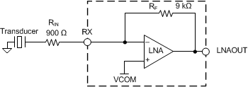 Figure 17. LNA Resistive Feedback Configuration
The LNA can be bypassed and disabled by writing a 1 to the LNA_CTRL bit in the TOF_1 register.
8.3.4 Programmable Gain Amplifier (PGA)
The PGA, shown in Figure 18, is an inverting amplifier with an input resistance of RIN = 500 Ω and a programmable feedback resistor RFB that can be programmed to set a 0-dB to 21-dB gain in 3-dB steps. This can be done by programming the PGA_GAIN field in the TOF_1 register. The bandwidth of the PGA is scaled based on its programmed gain. The typical bandwidth of the PGA with a 100-kΩ load to VCM and a 10-pF capacitor to ground are listed in Table 1.
Table 1. Typical PGA Bandwidth
| PGA_GAIN (Hex) | Gain (dB) | Bandwidth (MHz) |
|---|---|---|
| 0h | 0 | 19.0 |
| 1h | 3 | 16.8 |
| 2h | 6 | 14.4 |
| 3h | 9 | 12.3 |
| 4h | 12 | 10.0 |
| 5h | 15 | 8.2 |
| 6h | 18 | 6.6 |
| 7h | 21 | 5.0 |
The PGA can be bypassed and disabled by writing a 1 to the PGA_CTRL bit in the TOF_1 register. The output of the PGA should not be loaded directly with capacitances greater than 10 pF.
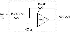 Figure 18. TDC1011 Programmable Gain Amplifier
8.3.5 Receiver Filters
It is recommended to place two filters in the RX path to minimize the receive path noise and obtain maximum timing accuracy. As shown in Figure 19, one filter is placed between the LNAOUT and the PGAIN pins, and another filter is placed between the PGAOUT and the COMPIN pins.
With an in-band gain of 10, the LNA has a bandwidth of 5 MHz. For most applications, a low-pass filter between the LNAOUT and PGAIN pins is sufficient.
As shown in Figure 19, the second filter stage can use a cascade of a low-pass filter (RF1 and CF3) followed by a high-pass filter (CF2 and RF2) referenced to VCOM. Design of the filter is straightforward. The RF1 and CF2 can be chosen first. A reasonable set of values for RF1 and CF2 could be: RF1 = 1 kΩ ± 10% and CF2 = 50pF ± 10%. Given the center frequency of interest to be ƒC and the filter bandwidth to be ƒB, the value of CF3 can be calculated as:

RF2 and CF2 determine the high-pass corner of the filter. RF2 should be referenced to VCOM to maintain the DC bias level at the comparator input during the echo receive time. For values of RF2 larger than RF1, there will be limited loading effect from the high-pass filter to the low-pass filter resulting in more accurate corner frequencies. The chosen values shown in the figure below result in a high-pass corner frequency of about 600 kHz and a low-pass corner frequency of about 3 MHz.
More complex filters can be used; external gain is acceptable if the signal amplitude is too low. If the pass-band of the filter is wider than an octave, it is recommended to use a filter design which has linear group delay.
 Figure 19. Filter for a 1-MHz Operation
8.3.6 Comparators for STOP Pulse Generation
The STOP pulse generation block of the TDC1011 contains two auto-zeroed comparators (a zero-cross detect and a threshold-detect comparator), a threshold setting DAC, and an event manager.
Comparator auto-zero periods occur at the beginning of every TOF receive cycle. During these periods, the comparator’s input offset is stored in an internal 2.5-pF capacitor, and it is subtracted from the input signal during the echo processing phase. The duration of auto-zero period is configured with the AUTOZERO_PERIOD field located in the CLOCK_RATE register.
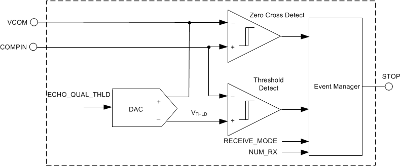 Figure 20. STOP Pulse Generation Circuit
8.3.6.1 Threshold Detector and DAC
The threshold detect comparator in Figure 20 compares the echo amplitude with a programmable threshold level (VTHLD) controlled by a DAC. The DAC voltage is set by the ECHO_QUAL_THLD field in register CONFIG_3 and provides 8 programmable threshold levels, VTHLD. The typical levels are summarized in Table 2:
Table 2. Echo Qualification Threshold Levels
| ECHO_QUAL_THLD | 0h | 1h | 2h | 3h | 4h | 5h | 6h | 7h |
| Typical VTHLD (mV) | –35 | –50 | –75 | –125 | –220 | –410 | –775 | –1500 |
8.3.6.2 Zero-cross Detect Comparator
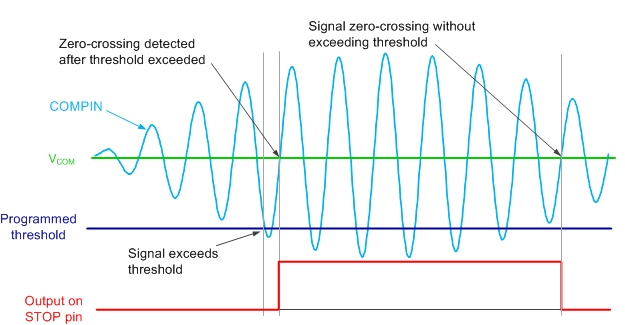
The zero-cross detect comparator compares the amplified echo signal at COMPIN with its reference voltage, which is VCOM. As shown in Figure 21, the comparator produces a low-to-high transition when the amplitude of the echo signal rises above VCOM. The comparator produces a high-to-low transition when the echo amplitude falls below VCOM – VHYST. The built-in negative-sided hysteresis of 10 mV in reference to VCOM ensures accurate zero-cross time instances associated with the rising edges of the echo signal and immunity of the comparator output to noise.
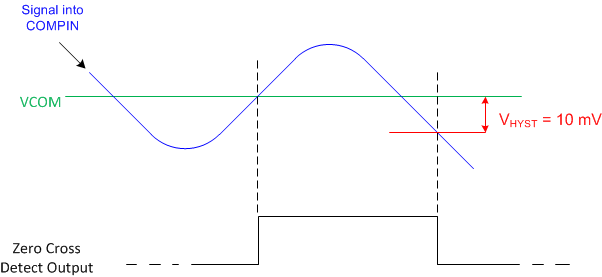 Figure 21. Zero-Cross Detector Output Signal
The output of the zero-cross detect comparator is passed to the event manager, where depending on the decision of the threshold-detect comparator.
8.3.6.3 Event Manager
The event manager is a digital state machine in the STOP pulse generation circuit of the TDC1011. The event manager controls the maximum number of STOP pulses to generate on the STOP pin and the receive mode for the STOP pulse generation. The number of STOP pulses is configured in the NUM_RX field in the CONFIG_1 register. The receive mode is selected in the RECEIVE_MODE bit of the CONFIG_4 register. See sections Single Echo Receive Mode and Multiple Echo Receive Mode for details about the receiver modes of the TDC1011.
An example for NUM_RX = 2h and RECEIVE_MODE = 0 is shown in Figure 22. When the echo signal amplitude exceeds values smaller than VTHLD, the threshold detect comparator indicates to the event manager to qualify the next zero-cross event as valid. When the qualified zero-cross is detected by the zero-cross detect comparator, the event manager passes the pulse to the STOP pin until the number of receive events programmed in NUM_RX is reached.
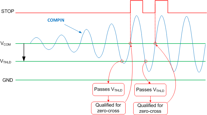 Figure 22. Signal Qualification, Zero-cross Detection and STOP Pulse Generation
8.3.7 Common-mode Buffer (VCOM)
The output of the internal common-mode buffer is present at the VCOM pin. This pin should be bypassed to ground with a low-leakage 10-nF capacitor and it should not be loaded with more than 20 µA. The common-mode buffer can be disabled with the VCOM_SEL bit in the CONFIG_2 register. If disabled, an external reference voltage must be applied to the VCOM pin.
During a time-of-flight measurement, the common-mode reference will take approximately 16 µs to settle if starting from zero initial conditions. Using a larger capacitor will increase the settling time of the internal common-mode reference. The implications of a larger VCOM capacitor are further explored in the Common-mode Reference Settling Time section.
8.3.8 Temperature Sensor
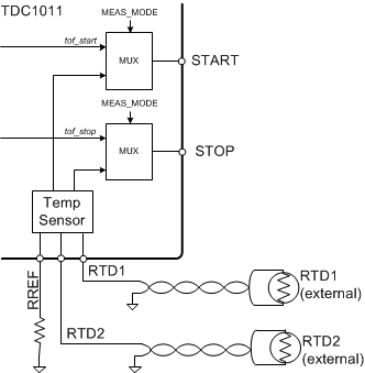 Figure 23. Temperature Sensor Measurement
Accurate measurements of level, and concentration may require compensation for the temperature dependency of the speed of sound in the medium. The TDC1011 provides two temperature sensor connections, allowing to measure up to two locations with RTDs, as shown in Figure 23.
The temperature sensor block supports PT1000 or PT500 sensors. The type of RTD used must be selected in the TEMP_RTD_SEL bit of the CONFIG_3 register. The system requires a temperature-stable external reference resistor (RREF). If the RTD type is PT500, then RREF should be 500 Ω. If the RTD type is PT1000, then RREF should be 1 kΩ. The reference resistor needs to have either a low temperature coefficient or be calibrated for temperature shift.
The logic timing in a temperature measurement is controlled by the TEMP_CLK_DIV bit in the CONFIG_3 register. As shown in Figure 24, the external clock can be divided by 8 or by the value resulting from the TX_FREQ_DIV field configuration in the CONFIG_0 register. It is recommended to operate the temperature measurement block at frequencies of 1 MHz or less.
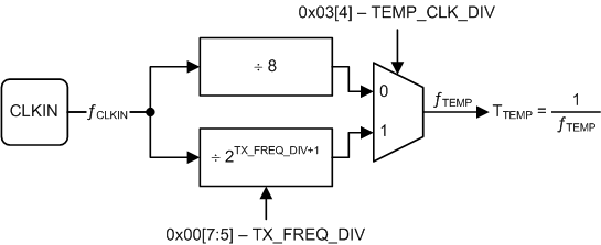 Figure 24. Timing Source for the Temperature Measurement
8.3.8.1 Temperature Measurement with Multiple RTDs
The temperature measurement mode is selected by setting the MEAS_MODE bit in the CONFIG_2 register to 1. A temperature measurement is started by sending a trigger pulse. After the temperature measurement is complete, the TDC1011 returns to SLEEP mode. To return to TOF measurement mode, reset the MEAS_MODE bit to 0.
The temperature sensor measurement can be performed without the need of an external ADC. The temperature sensor block operates by converting the resistance of a reference, RREF, and up to two RTDs into a series of START and STOP pulses. The interval between the pulses is proportional to the measured resistance, and therefore, the temperature. As shown in Figure 25, the TDC1011 performs three measurements per trigger event and generates the corresponding pulses on the START and STOP pins.
 Figure 25. Temperature Measurement Output Timing
The resistance of RTD1 and RTD2 can be calculated from the time intervals in Figure 25 as follows:

With a 1-kΩ reference resistor, the tREF interval is approximately 200 μs. The following intervals, tRTD1 and tRTD2, will depend on the resistance of the RTDs. The time delay between measurements, td1 and td2, can be approximated as follows:
For example, two PT1000 sensors at 0°C will have an approximate resistance of 1 kΩ; the same as the reference resistor in this example. Given an external 8-MHz clock and the default temperature clock divide-by-8 from the TEMP_CLK_DIV bit, the overall measurement time between the START pulse and the last STOP pulse is approximately 922 µs.
8.3.8.2 Temperature Measurement with a Single RTD
The temperature sensing block can be configured to measure a single RTD by setting the TEMP_MODE bit in register CONFIG_3 to 1. When the temperature measurement runs in PT1000 mode (TEMP_RTD_SEL = 0), the first interval corresponds to RREF, the second interval is a redundant measurement on RREF and should be neglected, and the third interval corresponds to RTD1. This operation is represented in Figure 26.
 Figure 26. Temperature Measurement with a Single PT1000
The resistance of RTD1 can be calculated using Equation 3. The time delay between measurements can be approximated using Equation 4 and Equation 5, with the exception that in this case, td1 is a function of ½ tREF and td2 is a function of tRTD1.
If the temperature measurement runs in PT500 mode (TEMP_RTD_SEL = 1), the first interval is a redundant measurement on RREF and should be neglected, the second interval corresponds to RREF, and the third interval corresponds to RTD1. This operation is represented in Figure 27.
 Figure 27. Temperature Measurement with a Single PT500
The resistance of RTD1 can be calculated using Equation 3. The time delay between measurements can be approximated using Equation 4 and Equation 5, with the exception that in this case, td1 is a function of tREF and td2 is a function of tRTD1.
8.4 Device Function Description
8.4.1 Time-of-Flight Measurement Mode
The TOF measurement mode is selected by setting the MEAS_MODE bit in the CONFIG_2 register to 0.
8.4.1.1 Liquid Level or Fluid Identification
The TDC1011 performs a single TOF measurement after receiving a trigger signal and returns to the SLEEP mode when the measurement is complete.
8.4.2 State Machine
A state machine in the TDC1011 manages the operation of the various measurement modes (see Figure 28). At power-on, the state machine is reset and most blocks are disabled. After the power-on sequence is complete, the device goes into SLEEP mode if the EN pin is low or into READY mode if the EN pin is high. In the SLEEP or READY state, the TDC1011 is able to receive SPI commands to set registers and configure the device for a measurement mode.
NOTE
Although the SPI block is always active, it is not recommended to perform configuration changes while the device is active. Configuration changes should be performed while the device is in the SLEEP state or in the READY state.
If the EN pin is high and a trigger signal is received, the state machine will begin the execution of the configured measurement. The state machine will return to the SLEEP state after the measurement is completed.
The device can be forced to exit a measurement by applying a logic high on the RESET pin high or a logic low on the EN pin.
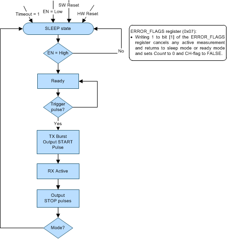 Figure 28. Simplified TDC1011 State Machine Diagram
8.4.3 TRANSMIT Operation
8.4.3.1 Transmission Pulse Count
The number of TX pulses generated by the TDC1011 to drive an ultrasonic transducer is programmable using the NUM_TX field located in the CONFIG_0 register.
8.4.3.2 TX 180° Pulse Shift
As shown in Figure 29, the transmitter block can add a 180° shift at a position in the TX signal. The position of the pulse shift is set by the TX_PH_SHIFT_POS field in the CONFIG_4 register and allows generating a specific signal pattern.
 Figure 29. Transmitter Pulse Signature, 180° Burst
As shown in Figure 30, enabling the TX 180° pulse shift has the effect of decreasing the number of transmitted pulses by 1.
 Figure 30. Transmitter Pulse Signature
In some cases, the 180° pulse shift may help improving the turn-off time of a transducer, and thus suppress the transmit ringing.
The 180° pulse shift is disabled by setting TX_PH_SHIFT_POS to position 31. Setting the 180° pulse shift to positions 0 or 1 is not recommended.
8.4.3.3 Transmitter Damping
The transmitter damping feature allows for improved control over the transducer signal generation. Damping extends the duration of the last TX pulse to help dissipate ringing and improve the transducer's turn-off time (see Figure 31 and Figure 32). The accuracy of measurements can be improved by having a faster transducer turn-off time. Damping is controlled with the DAMPING bit in the CONFIG_2 register.
 Figure 31. Transmitter Damping (5 Tx Pulses With a Damping Pulse)
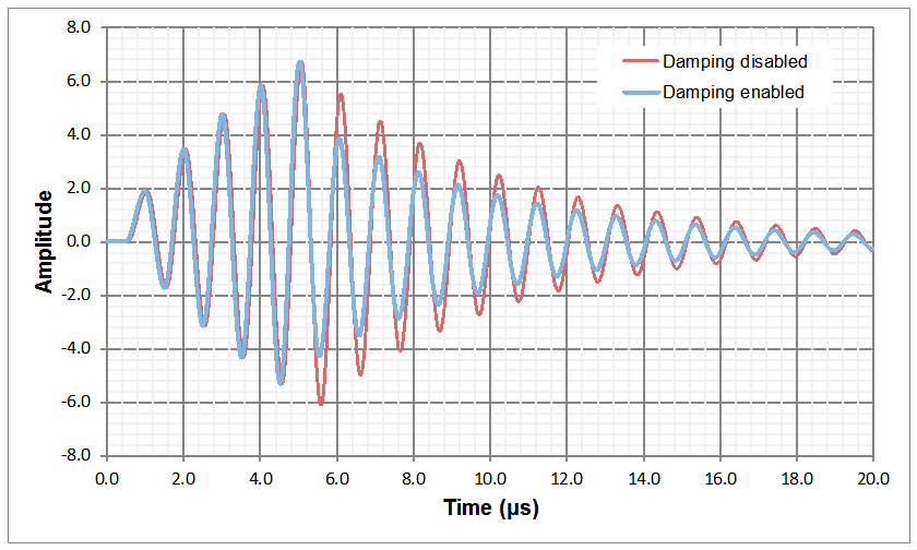 Figure 32. Transmitter Damped Echo
There are two invalid use combinations of the damping feature that may result in unexpected behavior. First, damping should not be combined with the 180° pulse shift described in the previous section. Second, damping should not be enabled if the number of TX pulses is set to 31.
8.4.4 RECEIVE Operation
8.4.4.1 Single Echo Receive Mode
Single Echo mode can be used for fluid identification measurements or level applications where transducer carrier frequency information is required. The device can be configured for Single Echo mode by setting the RECEIVE_MODE bit to 0 in the CONFIG_4 register. In Single Echo mode, the device will generate STOP pulses for every zero-cross qualified by the threshold comparator, up to the number of expected STOP events configured in the NUM_RX field in the CONFIG_1 register.
The threshold comparator qualifies the next zero-cross after an RX amplitude smaller than the programmed threshold voltage is detected. The zero-cross detector will provide output pulses corresponding to the rising edge of the received signal crossing the VCOM level, as shown in Figure 33. The threshold voltage can be set in the ECHO_QUAL_THDL field in the CONFIG_3 register.
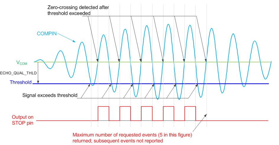 Figure 33. Single Echo Receive Mode (5 STOP Events)
If the number of expected pulses programmed in NUM_RX is not received or the time-of-flight operation times out, the TDC1011 will indicate an error condition in the ERROR_FLAGS register and will set the ERRB pin low.
8.4.4.2 Multiple Echo Receive Mode
The Multiple Echo mode is intended for use in level sensing applications and distance/displacement measurements in which multiple echoes (burst) are received. In this condition, each received echo group will be treated as a single pulse on the STOP pin. Up to 7 STOP pulses can be generated based on the value of the NUM_RX field in the CONFIG_1 register. Multi echo mode can be enabled by setting the RECEIVE_MODE bit to 1 in the CONFIG_4 register. A representation of multiple echo STOP pulse generation is shown in Figure 34.
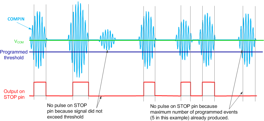 Figure 34. Multiple Echo Receive Mode (5 STOP Events)
The rising edge of a STOP pulse is generated by a zero-crossing event. As in the Single Echo Receive Mode, the threshold comparator qualifies the next zero-cross after an RX amplitude smaller than the programmed threshold voltage is detected. The STOP pulse will extend until a zero-cross after the RX amplitude is no longer smaller than the threshold voltage (see Figure 35).
If the number of expected pulses programmed in NUM_RX is not received or the time-of-flight operation times out, the TDC1011 will indicate an error condition in the ERROR_FLAGS register and will set the ERRB pin low.
8.4.5 Timing
8.4.5.1 Timing Control and Frequency Scaling (CLKIN)
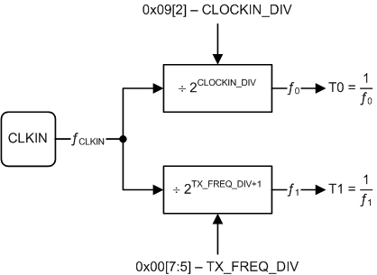 Figure 36. External Clock Division Tree
All transmit and receive function sequencing is synchronous to the external clock applied to the CLKIN pin. The external clock is divided to generate two internal clocks with corresponding time periods denoted as T0 and T1 in Figure 36. The division factor used to generate T0 is controlled with the CLOCKIN_DIV bit in the CLOCK_RATE register. The division factor used to generate T1 is controlled with the TX_FREQ_DIV field located in the CONFIG_0 register.
The SPI block is synchronous with the clock applied to the SCLK pin, and it is independent of the clock applied to CLKIN. See the Serial Peripheral Interface (SPI) section for a complete description of the SPI block.
8.4.5.2 TX/RX Measurement Sequencing and Timing
The TDC1011 automatically sequences the TX and RX functionality. After receiving a pulse edge on the TRIGGER pin, the TDC1011 resynchronizes to the CLKIN signal, and sends a TX burst.
The trigger edge polarity is configured to rising edge by default, but it can be changed to falling edge by setting the TRIG_EDGE_POLARITY bit in the CONFIG_4 register to 1.
After a device reset, the system must wait a determined time before sending the next trigger signal. The typical reset to trigger wait time is 3 × T1 + 50 ns.
8.4.6 Time-of-Flight (TOF) Control
The possible configurations of the TX/RX sequencing during a time-of-flight measurement can be divided into three cases: Short TOF Measurement, Standard TOF Measurement and Standard TOF Measurement with Power Blanking. Overall, the cases differ in the order of sequencing, power saving and echo listening windows. The behavior of each case is described in the sections to follow.
8.4.6.1 Short TOF Measurement
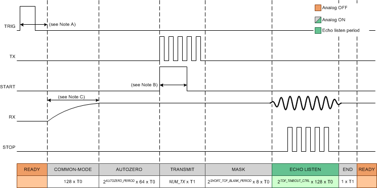
In a short time of flight measurement, the RX path is activated before the TX burst, as shown in Figure 37.
The short TOF is the default measurement sequence selected at power-on. The short TOF measurement is selected if the value of the TIMING_REG[9:0] field is less than 30, or if the FORCE_SHORT_TOF bit is set to 1. The TIMING_REG[9:0] is a 10-bit wide field, with its 2 most significant bits located in the TOF_1 register, and the 8 least significant bits located in the TOF_0 register. The FORCE_SHORT_TOF bit is located in the TIMEOUT register.
The comparator's input offset is stored in an internal capacitor during the auto-zero period. The length of the auto-zero period is controlled by the AUTOZERO_PERIOD field in the CLOCK_RATE register.
The length of the window when the comparators are able to qualify and generate STOP pulses is configured by the TOF_TIMEOUT_CTRL field. A timeout will occur if the number of expected pulses is not received during the allocated time and an error condition is reported to the ERROR_FLAGS register and the ERRB pin. It is possible to disable the echo timeout (see TOF Measurement Interval). The TOF_TIMEOUT_CTRL field is located in the TIMEOUT register.
See the Timing Control and Frequency Scaling (CLKIN) section for the definition of the time periods T0 and T1.
8.4.6.2 Standard TOF Measurement
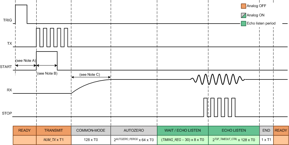
In a standard time of flight measurement, the RX path is activated after the TX burst is completed, as shown in Figure 38.
The standard TOF measurement sequence is enabled if the value of the TIMING_REG field is greater than or equal to 30, and only if the FORCE_SHORT_TOF bit is set to 0. The TIMING_REG is a 10-bit wide field, with its 2 most significant bits located in the TOF_1 register, and the 8 least significant bits located in the TOF_0 register. The FORCE_SHORT_TOF bit is located in the TIMEOUT register.
The comparator's input offset is stored in an internal capacitor during the auto-zero period. The length of the auto-zero period is controlled by the AUTOZERO_PERIOD field in the CLOCK_RATE register.
The length of the window when the comparators are able to qualify and generate STOP pulses is configured by a combination of the TIMING_REG field and the TOF_TIMEOUT_CTRL field. With the addition of the TIMING_REG in the calculation, the standard TOF measurement allows for a longer wait time and listening window. A timeout will occur if the number of expected pulses is not received during the allocated time and an error condition is reported to the ERROR_FLAGS register and the ERRB pin. It is possible to disable the echo timeout (see TOF Measurement Interval). The TOF_TIMEOUT_CTRL field is located in the TIMEOUT register.
NOTE
If the FORCE_SHORT_TOF bit = 1, the measurement sequencing will behave as a Short TOF Measurement, thus overriding the setting of the TIMING_REG field.
8.4.6.3 Standard TOF Measurement with Power Blanking
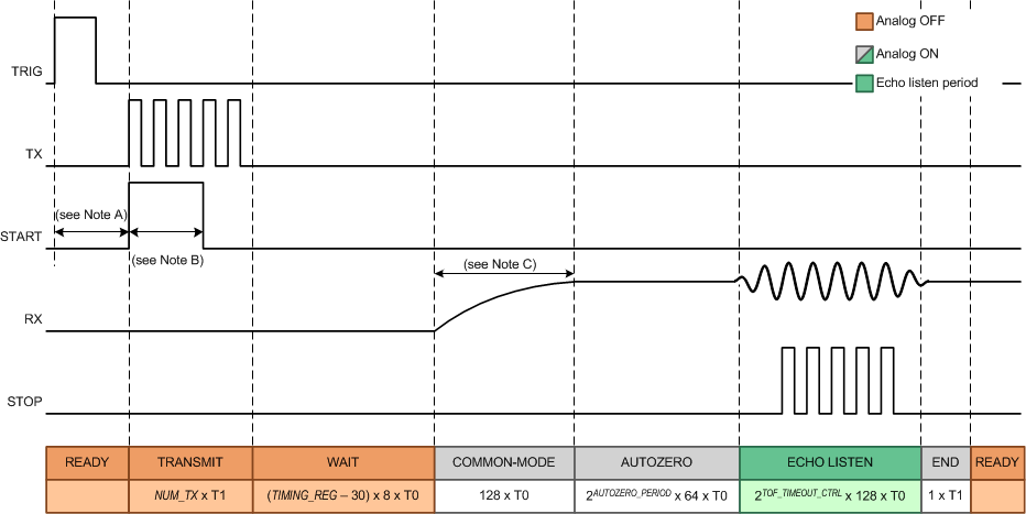
The power blanking sequence is a variation to the standard TOF measurement sequence, and can be enabled by setting the BLANKING bit to 1. In addition, all other conditions described in the Standard TOF Measurement should be met. The BLANKING bit can be found in the CONFIG_3 register.
Power blanking allows the device to remain in a low-power state while the TX signals propagate to the RX transducer in situations when the expected time-of-flight is long. Power blanking uses the TIMING_REG to control a wait time between the transmit sequence and the receive sequence, during which, the complete RX chain is disabled, as shown in Figure 39. The TIMING_REG is a 10-bit wide field, with its 2 most significant bits located in the TOF_1 register, and the 7 least significant bits located in the TOF_0 register.
8.4.6.4 Common-mode Reference Settling Time
The duration of the common-mode settling time is defined by the VCOM capacitor. With a 10-nF VCOM capacitor, the common-mode reference requires 16 µs to settle. On the other hand, the duration of the common-mode settling window is defined as 128 × T0, where the time unit T0 is determined by the external clock frequency and the value of the CLOCKIN_DIV bit, as explained in the Timing Control and Frequency Scaling (CLKIN) section.
A frequency of 8 MHz will result in a settling window of 128 × 1 / 8 MHz, which equals to 16 µs. Increasing the value of the VCOM capacitor will increase the common-mode settling time, but for the same 8-MHz frequency, the duration of the common-mode settling window will remain at 16 µs. In such situation, the common-mode reference will take multiple TOF cycles to reach its final value when starting from zero initial conditions.
8.4.6.5 TOF Measurement Interval
The comparators in the TDC1011's RX path can qualify and generate STOP pulses from a received echo within an interval set by the TOF_TIMEOUT_CTRL field in the TIMEOUT register. The listening interval can be extended in the standard TOF measurement (without blanking) by a period controlled with the TIMING_REG field (see Standard TOF Measurement).
If the number of STOP events programmed in the NUM_RX field is not received within the listening interval, a timeout event will occur and the device will return to the READY state. In addition, an error will be reported to the ERROR_FLAGS register and the ERRB pin will be driven low.
The echo timeout can be disabled by setting the ECHO_TIMEOUT bit to 1 in the TIMEOUT register. If the echo timeout is disabled, the device will not exit from the receive state until the expected number of STOP events set in NUM_RX occur. If the number of events does not occur, the device can be forced out of the receive state by writing a value of 0x03 to the ERROR_FLAGS register, or by de-asserting the EN pin, or asserting the RESET pin.
NOTE
Writing a logic 1 to bit [1] of the ERROR_FLAGS register clears the state machine. Writing a logic 1 to bit[0] clears the error flags.
NOTE
It is not recommended to hold the RX in an active state for intervals longer than 100ms, as the comparator auto-zero may no longer be accurate.
8.4.7 Error Reporting
The TDC1011 will report an error when the receive signals do not match the expected configuration. The ERRB pin will go low to indicate the presence of an error condition. Reading the ERROR_FLAGS register provides information about the condition(s) that caused the error.
The ERR_SIG_WEAK bit indicates that the number of received and qualified zero-crossings was less than the expected number set in the NUM_RX register field and a timeout occurred. This error is cleared when bit [0] is written to 1.
The ERR_NO_SIG bit indicates that no signals were received and a timeout occurred. Writing a 1 to this bit resets the state machine, halts active measurements and returns the device to SLEEP or READY mode. This error is cleared when bit [0] is written to 1.
The ERR_SIG_HIGH bit indicates that the received echo amplitude exceeds the largest echo qualification threshold at the input of the comparators. The ERR_SIG_HIGH error is only reported when the ECHO_QUAL_THDL register field is set to 7h. Writing a 1 to this bit will reset all the error flags and reset the ERRB pin to high.
NOTE
It is recommended to reset the state machine when the error flags are cleared. This can be done simultaneously by writing a value of 0x03 to the ERROR_FLAGS register.
8.5 Programming
8.5.1 Serial Peripheral Interface (SPI)
The serial interface consists of serial data input (SDI), serial data output (SDO), serial interface clock (SCLK) and chip select bar (CSB). The serial interface is used to configure the TDC1011 parameters available in various configuration registers. All the registers are organized into individually addressable byte-long registers with a unique address.
The communication on the SPI bus normally supports write and read transactions. A write transaction consists of a single write command byte, followed by single data byte. A read transaction consists of a single read command byte followed by 8 SCLK cycles. The write and read command bytes consist of 1 reserved bit, a 1-bit instruction, and a 6-bit register address. Figure 40 shows the SPI protocol for a transaction involving one byte of data (read or write).
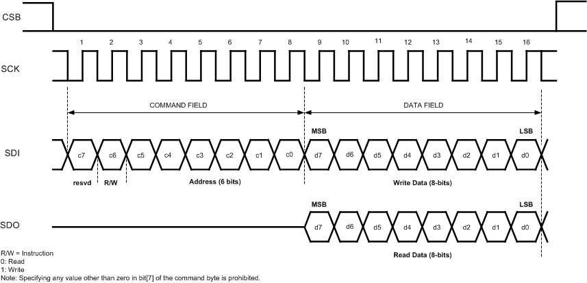 Figure 40. SPI Protocol
8.5.1.1 Chip Select Bar (CSB)
CSB is an active-low signal and needs to be low throughout a transaction. That is, CSB should not pulse between the command byte and the data byte of a single transaction.
De-asserting CSB always terminates an ongoing transaction, even if it is not yet complete. Re-asserting CSB will always bring the device into a state ready for the next transaction, regardless of the termination status of a previous transaction.
8.5.1.2 Serial Clock (SCLK)
SCLK can idle high or low. It is recommended to keep SCLK as clean as possible to prevent glitches from corrupting the SPI frame.
8.5.1.3 Serial Data Input (SDI)
SDI is driven by the SPI master by sending the command and the data byte to configure the AFE.
8.5.1.4 Serial Data Output (SDO)
SDO is driven by the AFE when the SPI master initiates a read transaction.
8.6 Register Maps
NOTE
- Reserved bits must be written to 0 unless otherwise indicated.
- Read-back value of reserved bits and registers is unspecified and should be discarded.
- Recommended values must be programmed and forbidden values must not be programmed where they are indicated to avoid unexpected results.
8.6.1 TDC1011 Registers
Table 3 list the memory-mapped registers for the TDC1011. All register addresses not listed in Table 3 should be considered as reserved locations and the register contents should not be modified.
Table 3. TDC1011 REGISTERS
| Address (Hex) | Acronym | Register Name | Reset Value | Section |
|---|---|---|---|---|
| 0h | CONFIG_0 | Config-0 | 45h | See here |
| 1h | CONFIG_1 | Config-1 | 40h | See here |
| 2h | CONFIG_2 | Config-2 | 0h | See here |
| 3h | CONFIG_3 | Config-3 | 3h | See here |
| 4h | CONFIG_4 | Config-4 | 1Fh | See here |
| 5h | TOF_1 | TOF-1 | 0h | See here |
| 6h | TOF_0 | TOF-0 | 0h | See here |
| 7h | ERROR_FLAGS | Error Flags | 0h | See here |
| 8h | TIMEOUT | Timeout | 19h | See here |
| 9h | CLOCK_RATE | Clock Rate | 0h | See here |
8.6.1.1 CONFIG_0 Register (address = 0h) [reset = 45h] (map)
| (MSB) 7 | 6 | 5 | 4 | 3 | 2 | 1 | 0 (LSB) |
| TX_FREQ_DIV | NUM_TX | ||||||
| R/W-2h | R/W-5h | ||||||
NOINDENT:
LEGEND: R/W = Read or write; R = Read only; R/W1C = Read or write 1 to clearTable 4. CONFIG_0 Register Field Descriptions
| Bit | Field | Type | Reset | Description |
|---|---|---|---|---|
| [7:5] | TX_FREQ_DIV(1) | R/W | 2h |
Frequency divider for TX clock and T1 0h: Divide by 2 1h: Divide by 4 2h: Divide by 8 (default) 3h: Divide by 16 4h: Divide by 32 5h: Divide by 64 6h: Divide by 128 7h: Divide by 256 |
| [4:0] | NUM_TX | R/W | 5h |
Number of TX pulses in a burst, ranging from 0 to 31. 5h: 5 pulses (default) |
8.6.1.2 CONFIG_1 Register (address = 1h) [reset = 40h] (map)
| (MSB) 7 | 6 | 5 | 4 | 3 | 2 | 1 | 0 (LSB) |
| RESERVED | RESERVED | NUM_RX | |||||
| R/W-1h | R/W-0h | R/W-0h | |||||
NOINDENT:
LEGEND: R/W = Read or write; R = Read only; R/W1C = Read or write 1 to clearTable 5. CONFIG_1 Register Field Descriptions
| Bit | Field | Type | Reset | Description |
|---|---|---|---|---|
| [7:6] | RESERVED | R/W | 1h |
1h: Reserved (default) |
| [5:3] | RESERVED | R/W | 0h | Must always be written 0h (default) |
| [2:0] | NUM_RX | R/W | 0h |
Number of expected receive events 0h: Do not count events (32 STOP pulses output) (default) 1h: 1 event (1 STOP pulse output) 2h: 2 events (2 STOP pulses output) 3h: 3 events (3 STOP pulses output) 4h: 4 events (4 STOP pulses output) 5h: 5 events (5 STOP pulses output) 6h: 6 events (6 STOP pulses output) 7h: 7 events (7 STOP pulses output) |
8.6.1.3 CONFIG_2 Register (address = 2h) [reset = 0h] (map)
| (MSB) 7 | 6 | 5 | 4 | 3 | 2 | 1 | 0 (LSB) |
| VCOM_SEL | MEAS_MODE | DAMPING | RESERVED | ||||
| R/W-0h | R/W-0h | R/W-0h | R/W-0h | ||||
NOINDENT:
LEGEND: R/W = Read or write; R = Read only; R/W1C = Read or write 1 to clearTable 6. CONFIG_2 Register Field Descriptions
| Bit | Field | Type | Reset | Description |
|---|---|---|---|---|
| [7] | VCOM_SEL | R/W | 0h |
Common-mode voltage reference control 0h: Internal (default) 1h: External |
| [6] | MEAS_MODE | R/W | 0h |
AFE measurement type 0h: Time-of-flight measurement (default) 1h: Temperature measurement |
| [5] | DAMPING | R/W | 0h |
TX burst damping 0h: Disable damping (default) 1h: Enable damping |
| [4:0] | RESERVED | R/W | 0h | Must always be written 0h (default) |
8.6.1.4 CONFIG_3 Register (address 3h) [reset = 3h] (map)
| (MSB) 7 | 6 | 5 | 4 | 3 | 2 | 1 | 0 (LSB) |
| RESERVED | TEMP_MODE | TEMP_RTD_SEL | TEMP_CLK_DIV | BLANKING | ECHO_QUAL_THLD | ||
| R/W-0h | R/W-0h | R/W-0h | R/W-0h | R/W-0h | R/W-3h | ||
NOINDENT:
LEGEND: R/W = Read or write; R = Read only; R/W1C = Read or write 1 to clearTable 7. CONFIG_3 Register Field Descriptions
| Bit | Field | Type | Reset | Description |
|---|---|---|---|---|
| [7] | RESERVED | R/W | 0h |
0h: Reserved (default) |
| [6] | TEMP_MODE | R/W | 0h |
Temperature measurement channels 0h: Measure REF, RTD1 and RTD2 (default) 1h: Measure REF and RTD1 |
| [5] | TEMP_RTD_SEL | R/W | 0h |
RTD type 0h: PT1000 (default) 1h: PT500 |
| [4] | TEMP_CLK_DIV | R/W | 0h |
Clock divider for temperature mode 0h: Divide by 8 (default) 1h: Use TX_FREQ_DIV |
| [3] | BLANKING | R/W | 0h |
Power blanking in standard TOF measurements. The blanking length is controlled with the TIMING_REG field (see Standard TOF Measurement with Power Blanking). 0h: Disable power blanking (default) 1h: Enable power blanking |
| [2:0] | ECHO_QUAL_THLD | R/W | 3h |
Echo qualification DAC threshold level with respect to VCOM 0h: –35 mV 1h: –50 mV 2h: –75 mV 3h: –125 mV (default) 4h: –220 mV 5h: –410 mV 6h: –775 mV 7h: –1500 mV |
8.6.1.5 CONFIG_4 Register (address = 4h) [reset = 1Fh] (map)
| (MSB) 7 | 6 | 5 | 4 | 3 | 2 | 1 | 0 (LSB) |
| RESERVED | RECEIVE_ MODE |
TRIG_EDGE_ POLARITY |
TX_PH_SHIFT_POS | ||||
| R/W-0h | R/W-0h | R/W-0h | R/W-1Fh | ||||
NOINDENT:
LEGEND: R/W = Read or write; R = Read only; R/W1C = Read or write 1 to clearTable 8. CONFIG_4 Register Field Descriptions
| Bit | Field | Type | Reset | Description |
|---|---|---|---|---|
| [7] | RESERVED | R/W | 0h |
0h: Reserved (default) |
| [6] | RECEIVE_MODE | R/W | 0h |
Receive echo mode 0h: Single echo (default) 1h: Multi echo |
| [5] | TRIG_EDGE_POLARITY | R/W | 0h |
Trigger edge polarity 0h: Rising edge (default) 1h: Falling edge |
| [4:0] | TX_PH_SHIFT_POS | R/W | 1Fh |
TX 180° pulse shift position, ranging from 0 to 31. 1Fh: Position 31 (default) It is not recommended to set TX_PH_SHIFT_POS to 0 or 1. |
8.6.1.6 TOF_1 Register (address = 5h) [reset = 0h] (map)
| (MSB) 7 | 6 | 5 | 4 | 3 | 2 | 1 | 0 (LSB) |
| PGA_GAIN | PGA_CTRL | LNA_CTRL | LNA_FB | TIMING_REG[9:8] | |||
| R/W-0h | R/W-0h | R/W-0h | R/W-0h | R/W-0h | |||
NOINDENT:
LEGEND: R/W = Read or write; R = Read only; R/W1C = Read or write 1 to clearTable 9. TOF_1 Register Field Descriptions
| Bit | Field | Type | Reset | Description |
|---|---|---|---|---|
| [7:5] | PGA_GAIN | R/W | 0h |
PGA gain 0h: 0 dB (default) 1h: 3 dB 2h: 6 dB 3h: 9 dB 4h: 12 dB 5h: 15 dB 6h: 18 dB 7h: 21 dB |
| [4] | PGA_CTRL | R/W | 0h |
PGA control 0h: Active (default) 1h: Bypassed and powered off |
| [3] | LNA_CTRL | R/W | 0h |
LNA control 0h: Active (default) 1h: Bypassed and powered off |
| [2] | LNA_FB | R/W | 0h |
LNA feedback mode 0h: Capacitive feedback (default) 1h: Resistive feedback |
| [1:0] | TIMING_REG[9:8] | R/W | 0h |
TIMING_REG field's 2 most-significant bits (see Standard TOF Measurement and Standard TOF Measurement with Power Blanking) 0h: 0 (default) |
8.6.1.7 TOF_0 Register (address = 6h) [reset = 0h] (map)
| (MSB) 7 | 6 | 5 | 4 | 3 | 2 | 1 | 0 (LSB) |
| TIMING_REG[7:0] | |||||||
| R/W-0h | |||||||
NOINDENT:
LEGEND: R/W = Read or write; R = Read only; R/W1C = Read or write 1 to clearTable 10. TOF_0 Register Field Descriptions
| Bit | Field | Type | Reset | Description |
|---|---|---|---|---|
| [7:0] | TIMING_REG[7:0] | R/W | 0h |
TIMING_REG field's 8 least-significant bits (see Standard TOF Measurement and Standard TOF Measurement with Power Blanking) 0h: 0 (default) |
8.6.1.8 ERROR_FLAGS Register (address = 7h) [reset = 0h] (map)
| 7 (MSB) | 6 | 5 | 4 | 3 | 2 | 1 | 0 (LSB) |
| RESERVED | ERR_ SIG_WEAK |
ERR_NO_SIG | ERR_ SIG_HIGH |
||||
| R-0h | R-0h | R/W1C-0 | R/W1C-0 | ||||
NOINDENT:
LEGEND: R/W = Read or write; R = Read only; R/W1C = Read or write 1 to clearTable 11. ERROR_FLAGS Register Field Descriptions(1)(2)
| Bit | Field | Type | Reset | Description |
|---|---|---|---|---|
| [7:3] | RESERVED | R | 0h |
0h: Reserved (default) |
| [2] | ERR_SIG_WEAK | R | 0h |
1h: The number of received and qualified zero-crossings was less than the expected number set in NUM_RX field and a timeout occurred. |
| [1] | ERR_NO_SIG | R/W1C | 0h |
1h: No signals were received and timeout occurred. Writing a 1 to this field resets the state machine, halts active measurements and returns the device to the SLEEP or READY mode. |
| [0] | ERR_SIG_HIGH | R/W1C | 0h |
1h: The received echo amplitude exceeds the largest echo qualification threshold at the input of the comparators. The error is only reported when ECHO_QUAL_THLD = 0x07. Writing a 1 to this field will reset all the error flags and reset the ERRB pin to high. |
8.6.1.9 TIMEOUT Register (address = 8h) [reset = 19h] (map)
| (MSB) 7 | 6 | 5 | 4 | 3 | 2 | 1 | 0 (LSB) |
| RESERVED | FORCE_ SHORT_TOF |
SHORT_TOF_BLANK_PERIOD | ECHO_ TIMEOUT |
TOF_TIMEOUT_CTRL | |||
| R/W-0h | R/W-0h | R/W-3h | R/W-0h | R/W-1h | |||
NOINDENT:
LEGEND: R/W = Read or write; R = Read only; R/W1C = Read or write 1 to clearTable 12. TIMEOUT Register Field Descriptions
| Bit | Field | Type | Reset | Description |
|---|---|---|---|---|
| [7] | RESERVED | R/W | 0h |
0h: Reserved (default) |
| [6] | FORCE_SHORT_TOF | R/W | 0h |
Short time-of-flight control 0h: Disabled (default) 1h: Force a short time-of-flight measurement |
| [5:3] | SHORT_TOF_BLANK_PERIOD(1) | R/W | 3h |
Short time-of-flight blanking period (see Short TOF Measurement) 0h: 8 × T0 1h: 16 × T0 2h: 32 × T0 3h: 64 × T0 (default) 4h: 128 × T0 5h: 256 × T0 6h: 512 × T0 7h: 1024 × T0 |
| [2] | ECHO_TIMEOUT | R/W | 0h |
Echo receive timeout control (see TOF Measurement Interval) 0h: Enable echo timeout (default) 1h: Disable timeout |
| [1:0] | TOF_TIMEOUT_CTRL(1) | R/W | 1h |
Echo listening window timeout (see TOF Measurement Interval) 0h: 128 × T0 1h: 256 × T0 (default) 2h: 512 × T0 3h: 1024 × T0 |
8.6.1.10 CLOCK_RATE Register (address = 9h) [reset = 0h] (map)
| (MSB) 7 | 6 | 5 | 4 | 3 | 2 | 1 | 0 (LSB) |
| RESERVED | CLOCKIN_DIV | AUTOZERO_PERIOD | |||||
| R/W-0h | R/W-0h | R/W-0h | |||||
NOINDENT:
LEGEND: R/W = Read or write; R = Read only; R/W1C = Read or write 1 to clearTable 13. CLOCK_RATE Register Field Descriptions(1)
| Bit | Field | Type | Reset | Description |
|---|---|---|---|---|
| [7:3] | RESERVED | R/W | 0h |
0h: Reserved (default) |
| [2] | CLOCKIN_DIV(1) | R/W | 0h |
CLKIN divider to generate T0 0h: Divide by 1 (default) 1h: Divide by 2 |
| [1:0] | AUTOZERO_PERIOD(1) | R/W | 0h |
Receiver auto-zero period 0h: 64 × T0 (default) 1h: 128 × T0 2h: 256 × T0 3h: 512 × T0 |
