JAJSLG2A April   2021  – September 2023 TDES960

PRODUCTION DATA  

  1.   1
  2. 特長
  3. アプリケーション
  4. 概要
  5. Revision History
  6. Pin Configuration and Functions
  7. Specifications
    1. 6.1  Absolute Maximum Ratings
    2. 6.2  ESD Ratings
    3. 6.3  Recommended Operating Conditions
    4. 6.4  Thermal Information
    5. 6.5  DC Electrical Characteristics
    6. 6.6  AC Electrical Characteristics
    7. 6.7  CSI-2 Timing Specifications
    8. 6.8  Recommended Timing for the Serial Control Bus
    9. 6.9  Timing Diagrams
    10. 6.10 Typical Characteristics
  8. Detailed Description
    1. 7.1 Overview
      1. 7.1.1 Functional Description
    2. 7.2 Functional Block Diagram
    3. 7.3 Feature Description
    4. 7.4 Device Functional Modes
      1. 7.4.1  CSI-2 Mode
      2. 7.4.2  RAW Mode
      3. 7.4.3  MODE Pin
      4. 7.4.4  REFCLK
      5. 7.4.5  Receiver Port Control
        1. 7.4.5.1 Video Stream Forwarding
      6. 7.4.6  Input Jitter Tolerance
      7. 7.4.7  Adaptive Equalizer
        1. 7.4.7.1 Channel Requirements
        2. 7.4.7.2 Adaptive Equalizer Algorithm
        3. 7.4.7.3 AEQ Settings
          1. 7.4.7.3.1 AEQ Start-Up and Initialization
          2. 7.4.7.3.2 AEQ Range
          3. 7.4.7.3.3 AEQ Timing
          4. 7.4.7.3.4 AEQ Threshold
      8. 7.4.8  Channel Monitor Loop-Through Output Driver
        1. 7.4.8.1 Code Example for CMLOUT V3LINK RX Port 0:
      9. 7.4.9  RX Port Status
        1. 7.4.9.1 RX Parity Status
        2. 7.4.9.2 V3Link Decoder Status
        3. 7.4.9.3 RX Port Input Signal Detection
        4. 7.4.9.4 Line Counter
        5. 7.4.9.5 Line Length
      10. 7.4.10 Sensor Status
      11. 7.4.11 GPIO Support
        1. 7.4.11.1 GPIO Input Control and Status
        2. 7.4.11.2 GPIO Output Pin Control
        3. 7.4.11.3 Forward Channel GPIO
        4. 7.4.11.4 Back Channel GPIO
        5. 7.4.11.5 GPIO Pin Status
        6. 7.4.11.6 Other GPIO Pin Controls
      12. 7.4.12 RAW Mode LV / FV Controls
      13. 7.4.13 CSI-2 Protocol Layer
      14. 7.4.14 CSI-2 Short Packet
      15. 7.4.15 CSI-2 Long Packet
      16. 7.4.16 CSI-2 Data Identifier
      17. 7.4.17 Virtual Channel and Context
      18. 7.4.18 CSI-2 Mode Virtual Channel Mapping
        1. 7.4.18.1 Example 1
        2. 7.4.18.2 Example 2
      19. 7.4.19 CSI-2 Transmitter Frequency
      20. 7.4.20 CSI-2 Output Bandwidth
        1. 7.4.20.1 CSI-2 Output Bandwidth Calculation Example
      21. 7.4.21 CSI-2 Transmitter Status
      22. 7.4.22 Video Buffers
      23. 7.4.23 CSI-2 Line Count and Line Length
      24. 7.4.24 FrameSync Operation
        1. 7.4.24.1 External FrameSync Control
        2. 7.4.24.2 Internally Generated FrameSync
          1. 7.4.24.2.1 Code Example for Internally Generated FrameSync
      25. 7.4.25 CSI-2 Forwarding
        1. 7.4.25.1 Best-Effort Round Robin CSI-2 Forwarding
        2. 7.4.25.2 Synchronized CSI-2 Forwarding
        3. 7.4.25.3 Basic Synchronized CSI-2 Forwarding
          1. 7.4.25.3.1 Code Example for Basic Synchronized CSI-2 Forwarding
        4. 7.4.25.4 Line-Interleaved CSI-2 Forwarding
          1. 7.4.25.4.1 Code Example for Line-Interleaved CSI-2 Forwarding
        5. 7.4.25.5 Line-Concatenated CSI-2 Forwarding
          1. 7.4.25.5.1 Code Example for Line-Concatenated CSI-2 Forwarding
        6. 7.4.25.6 CSI-2 Replicate Mode
        7. 7.4.25.7 CSI-2 Transmitter Output Control
        8. 7.4.25.8 Enabling and Disabling CSI-2 Transmitters
    5. 7.5 Programming
      1. 7.5.1  Serial Control Bus
      2. 7.5.2  Second I2C Port
      3. 7.5.3  I2C Target Operation
      4. 7.5.4  Remote Target Operation
      5. 7.5.5  Remote Target Addressing
      6. 7.5.6  Broadcast Write to Remote Devices
        1. 7.5.6.1 Code Example for Broadcast Write
      7. 7.5.7  I2C Controller Proxy
      8. 7.5.8  I2C Controller Proxy Timing
        1. 7.5.8.1 Code Example for Configuring Fast-Mode Plus I2C Operation
      9. 7.5.9  Interrupt Support
        1. 7.5.9.1 Code Example to Enable Interrupts
        2. 7.5.9.2 V3Link Receive Port Interrupts
        3. 7.5.9.3 Interrupts on Forward Channel GPIO
        4. 7.5.9.4 Interrupts on Change in Sensor Status
        5. 7.5.9.5 Code Example to Readback Interrupts
        6. 7.5.9.6 CSI-2 Transmit Port Interrupts
      10. 7.5.10 Error Handling
        1. 7.5.10.1 Receive Frame Threshold
        2. 7.5.10.2 Port PASS Control
      11. 7.5.11 Timestamp – Video Skew Detection
      12. 7.5.12 Pattern Generation
        1. 7.5.12.1 Reference Color Bar Pattern
        2. 7.5.12.2 Fixed Color Patterns
        3. 7.5.12.3 Pattern Generator Programming
          1. 7.5.12.3.1 Determining Color Bar Size
        4. 7.5.12.4 Code Example for Pattern Generator
      13. 7.5.13 V3Link BIST Mode
        1. 7.5.13.1 BIST Operation
    6. 7.6 Register Maps
      1. 7.6.1 Main Registers
      2. 7.6.2 Indirect Access Registers
        1. 7.6.2.1 PATGEN_And_CSI-2 Registers
  9. Application and Implementation
    1. 8.1 Application Information
      1. 8.1.1 Power Over Coax
    2. 8.2 Typical Application
      1. 8.2.1 Design Requirements
      2. 8.2.2 Detailed Design Procedure
      3. 8.2.3 Application Curves
    3. 8.3 System Examples
    4. 8.4 Power Supply Recommendations
      1. 8.4.1 VDD Power Supply
      2. 8.4.2 Power-Up Sequencing
        1. 8.4.2.1 PDB Pin
        2. 8.4.2.2 System Initialization
    5. 8.5 Layout
      1. 8.5.1 Layout Guidelines
        1. 8.5.1.1 Ground
        2. 8.5.1.2 Routing V3Link Signal Traces and PoC Filter
        3. 8.5.1.3 CSI-2 Guidelines
      2. 8.5.2 Layout Example
  10. Device and Documentation Support
    1. 9.1 Documentation Support
      1. 9.1.1 Related Documentation
    2. 9.2 Receiving Notification of Documentation Updates
    3. 9.3 サポート・リソース
    4. 9.4 Trademarks
    5. 9.5 静電気放電に関する注意事項
    6. 9.6 用語集
  11. 10Mechanical, Packaging, and Orderable Information

パッケージ・オプション

メカニカル・データ(パッケージ|ピン)
サーマルパッド・メカニカル・データ
発注情報

CSI-2 Data Identifier

The TDES960 MIPI CSI-2 protocol interface transmits the data identifier byte containing the values for the virtual channel ID (VC) and data type (DT) for the application specific payload data, as shown in Figure 7-9. The virtual channel ID is contained in the 2 MSBs of the data identifier byte and identify the data as directed to one of four virtual channels. The value of the data type is contained in the 6 LSBs of the data identifier byte. When partnered with the TSER953 serializer, the Data Type is passed through from the received CSI-2 packets. When partnered with a DVP Mode serializer, the received RAW mode data is converted to CSI-2 Tx packets with assigned data type and virtual channel ID.

For each RX Port, register defines with which channel and data type the context is associated:

  • For V3Link Receiver port operating in RAW input mode connected to a DVP Mode serializer, register 0x70 describes RAW10 Mode and 0x71 RAW12 Mode.
  • RAW1x_VC[7:6] field defines the associated virtual ID transported by the CSI-2 protocol from the camera sensor.
  • RAW1x_ID[5:0] field defines the associated data type. The data type is a combination of the data type transported by the CSI-2 protocol.
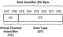
GUID-304C190E-C9D1-42FB-A699-33CF686A3620-low.gifFigure 7-9 CSI-2 Data Identifier Structure