JAJSOW0A July 2022 – July 2023 TDP1204
PRODUCTION DATA
- 1
- 1 特長
- 2 アプリケーション
- 3 概要
- 4 Revision History
- 5 Pin Configuration and Functions
- 6 Specifications
- 7 Parameter Measurement Information
-
8 Detailed Description
- 8.1 Functional Block Diagram
- 8.2
Feature Description
- 8.2.1 4-Level Inputs
- 8.2.2 I/O Voltage Level Selection
- 8.2.3 HPD_OUT
- 8.2.4 Lane Control
- 8.2.5 Swap
- 8.2.6 Linear and Limited Redriver
- 8.2.7 Main Link Inputs
- 8.2.8 Receiver Equalizer
- 8.2.9 CTLE Bypass
- 8.2.10 Adaptive Equalization in HDMI 2.1 FRL
- 8.2.11 HDMI 2.1 Link Training Compatible Rx EQ
- 8.2.12 Input Signal Detect
- 8.2.13 Main Link Outputs
- 8.2.14 DDC Buffer
- 8.2.15 HDMI DDC Capacitance
- 8.2.16 DisplayPort
- 8.3
Device Functional Modes
- 8.3.1
MODE Control
- 8.3.1.1 I2C Mode (MODE = "F")
- 8.3.1.2
Pin Strap Modes
- 8.3.1.2.1 Pin-Strap: HDMI 1.4 and HDMI 2.0 Functional Description
- 8.3.1.2.2 Pin-Strap HDMI 2.1 Function (MODE = "0"): Fixed Rx EQ and DDC Buffer Enabled
- 8.3.1.2.3 Pin-Strap HDMI 2.1 Function (MODE = "1"): Flexible RX EQ and DDC Buffer Enabled
- 8.3.1.2.4 Pin-Strap HDMI 2.1 Function (MODE = "R"): Flexible Rx EQ and DDC Buffer Disabled
- 8.3.2 DDC Snoop Feature
- 8.3.3 Low Power States
- 8.3.1
MODE Control
- 8.4 Programming
- 8.5 Register Maps
- 9 Application and Implementation
- 10デバイスおよびドキュメントのサポート
- 11Mechanical, Packaging, and Orderable Information
7 Parameter Measurement Information
 Figure 7-1 Power-On Timing
Requirements
 Figure 7-2 TMDS Main Link Test
Circuit
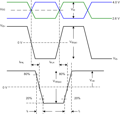 Figure 7-3 Input or Output Timing
Measurements
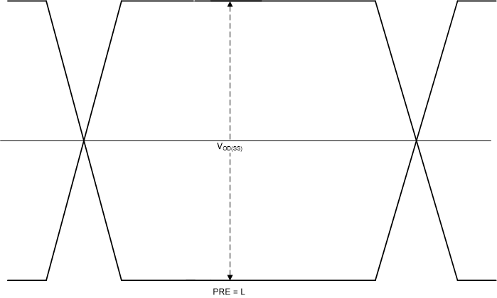 Figure 7-4 Output Differential
Waveform
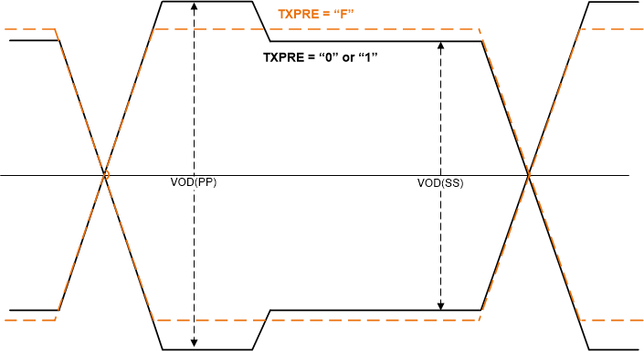 Figure 7-5 Output Differential
Waveform with De-Emphasis
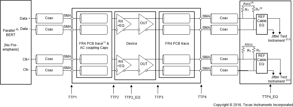
(1) The FR4
trace between TTP1 and TTP2 is designed to emulate 1-12” of FR4, AC-coupling
capacitor, connector and another 2” of FR4. Trace width – 4 mils. 100 Ω
differential impedance.
(2) All
Jitter is measured at a BER of 109. HDMI 2.1 jitter measured at BER 10-10.
(3) Residual
jitter reflects the total jitter measured at TTP4 minus the jitter measured
at TTP
(4) AVCC =
3.3 V.
(5)
RT = 50 Ω.
(6) For HDMI
1.4 or 2.0, the input signal from parallel Bert does not have any
pre-emphasis or de-emphasis. For HDMI 2.1 FRL, the input signal from BERT will have 2.18 dB
pre-shoot and −3.1 dB de-emphasis. Refer to Recommended
Operating Conditions.
Figure 7-6 HDMI Output Jitter
Measurement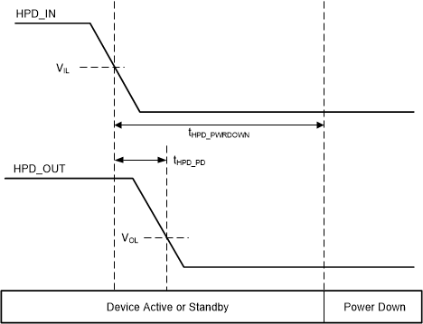 Figure 7-7 HPD Logic Shutdown and
Propagation Timing
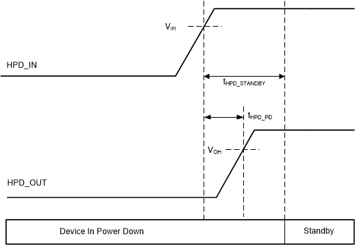 Figure 7-8 HPD Logic Standby and
Propagation Timing
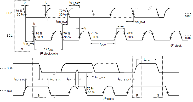 Figure 7-9 I2C SCL and SDA
Timing
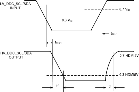 Figure 7-10 DDC Propagation Delay –
Source to Sink
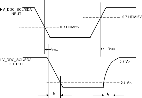 Figure 7-11 DDC Propagation Delay –
Sink to Source
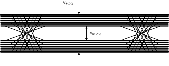 Figure 7-12 VID(DC) and
VID(EYE)