JAJSO92B November 2012 – March 2022 TFP401A-Q1
PRODUCTION DATA
- 1 特長
- 2 アプリケーション
- 3 概要
- 4 Revision History
- 5 Pin Configuration and Functions
-
6 Specifications
- 6.1 Absolute Maximum Ratings
- 6.2 ESD Ratings
- 6.3 Recommended Operating Conditions
- 6.4 Thermal Information
- 6.5 DC Digital I/O Electrical Characteristics
- 6.6 DC Electrical Characteristics
- 6.7 AC Electrical Characteristics
- 6.8 Timing Requirements
- 6.9 Switching Characteristics
- 6.10 Typical Characteristics
- 7 Detailed Description
- 8 Application and Implementation
- 9 Device and Documentation Support
- 10Mechanical, Packaging, and Orderable Information
パッケージ・オプション
メカニカル・データ(パッケージ|ピン)
- PZP|100
サーマルパッド・メカニカル・データ
- PZP|100
発注情報
6.8 Timing Requirements
| PARAMETER | TEST CONDITIONS | MIN | TYP | MAX | UNIT | ||
|---|---|---|---|---|---|---|---|
| tps | Analog input intra-pair (+ to –) differential skew (2) | 0.4 | tbit(1) | ||||
| tccs | Analog input inter-pair or channel-to-channel skew (2) | 1 | tpix(3) | ||||
| tijit | Worst-case differential input-clock jitter tolerance(2)(4) | 50 | ps | ||||
| tf1 | Fall time of data and control signals(5)(6) | ST = low, CL = 5 pF | 2.4 | ns | |||
| ST = high, CL = 10 pF | 1.9 | ||||||
| tr1 | Rise time of data and control signals(5)(6) | ST = low, CL = 5 pF | 2.4 | ns | |||
| ST = high, CL = 10 pF | 1.9 | ||||||
| tr2 | Rise time of ODCK clock(5) | ST = low, CL = 5 pF | 2.4 | ns | |||
| ST = high, CL = 10 pF | 1.9 | ||||||
| tf2 | Fall time of ODCK clock(5) | ST = low, CL = 5 pF | 2.4 | ns | |||
| ST = high, CL = 10 pF | 1.9 | ||||||
| tsu1 | Setup time, data and control signal to falling edge of ODCK | 1 pixel per clock, PIXS = low, OCK_INV = low | 1.8 | ns | |||
| 2 pixels per clock, PIXS = high, STAG = high, OCK_INV = low | 3.8 | ||||||
| 2 pixels and STAG, PIXS = high, STAG = low, OCK_INV = low | 0.6 | ||||||
| th1 | Hold time, data and control signal to falling edge of ODCK | 1 pixel per clock, PIXS = low, OCK_INV = low | 0.6 | ns | |||
| 2 pixels and STAG, PIXS = high, STAG = low, OCK_INV = low | 2.5 | ||||||
| 2 pixels per clock, PIXS = high, STAG = high, OCK_INV = low | 2.9 | ||||||
| tsu2 | Setup time, data and control signal to rising edge of ODCK | 1 pixels per clock, PIXS = low, OCK_INV = high | 2.1 | ns | |||
| 2 pixels per clock, PIXS = high, STAG = high, OCK_INV = high | 4 | ||||||
| 2 pixels and STAG, PIXS = high, STAG = low, OCK_INV = high | 1.5 | ||||||
| th2 | Hold time, data and control signal to rising edge of ODCK | 1 pixel per clock, PIXS = low, OCK_INV = high | 0.3 | ns | |||
| 2 pixels and STAG, PIXS = high, STAG = low, OCK_INV = high | 2.4 | ||||||
| 2 pixels per clock, PIXS = high, STAG = high, OCK_INV = high | 2.1 | ||||||
| tpix | Pixel time(3) | 6.06 | 40 | ns | |||
(1) tbit is 1/10 the pixel time, tpix.
(2) Specified by characterization.
(3) tpix is the pixel time defined as the period of the RxC clock input. The period of the output clock, ODCK, is equal to tpix when in 1-pixel-per-clock mode or 2 tpix when in 2-pixels-per-clock mode.
(4) Measured differentially at 50% crossing using ODCK output clock as
trigger.
(5) Rise and fall times measured as time between 20% and 80% of signal
amplitude.
(6) Data and control signals are QE[23:0], QO[23:0], DE, HSYNC, VSYNC. and CTL[3:1].
(7) Amount of time detected between DE transitions determines whether link is active or inactive. SCDT indicates link activity.
 Figure 6-1 Rise and Fall Times of Data and Control Signals
 Figure 6-2 Rise and Fall Times of ODCK
 Figure 6-3 ODCK Frequency
 Figure 6-4 Data Setup and Hold Times to Rising and Falling Edges of ODCK
![ODCK High to QE[23:0] Staggered Data Output GUID-DA37585F-0460-4604-982E-05A97D64DFE3-low.gif](/ods/images/JAJSO92B/GUID-DA37585F-0460-4604-982E-05A97D64DFE3-low.gif) Figure 6-5 ODCK High to QE[23:0] Staggered Data Output
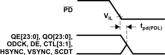
Figure 6-5 ODCK High to QE[23:0] Staggered Data Output Figure 6-6 Delay From
PD Low to Hi-Z Outputs
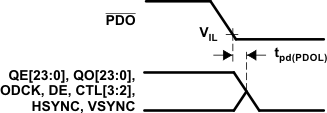
 Figure 6-7 Delay From
PDO Low to Hi-Z Outputs
 Figure 6-8 Delay From
PD Low to High Until Inputs Are Active
 Figure 6-9 Time From DE Transitions to SCDT Low and SCDT High