JAJST56D October 2001 – February 2024 TFP410
PRODUCTION DATA
- 1
- 1 特長
- 2 アプリケーション
- 3 概要
- 4 Pin Configuration and Functions
- 5 Specifications
-
6 Detailed Description
- 6.1 Overview
- 6.2 Functional Block Diagram
- 6.3 Feature Description
- 6.4 Device Functional Modes
- 6.5 Programming
- 6.6
Register Maps
- 6.6.1 VEN_ID Register (Sub-Address = 01−00 ) [reset = 0x014C]
- 6.6.2 DEV_ID Register (Sub-Address = 03–02) [reset = 0x0410]
- 6.6.3 REV_ID Register (Sub-Address = 04) [reset = 0x00]
- 6.6.4 Reserved Register (Sub-Address = 07–05) [reset = 0x641400]
- 6.6.5 CTL_1_MODE (Sub-Address = 08) [reset = 0xBE]
- 6.6.6 CTL_2_MODE Register (Sub-Address = 09) [reset = 0x00]
- 6.6.7 CTL_3_MODE Register (Sub-Address = 0A) [reset = 0x80]
- 6.6.8 CFG Register (Sub-Address = 0B)
- 6.6.9 RESERVED Register (Sub-Address = 0E–0C) [reset = 0x97D0A9]
- 6.6.10 DE_DLY Register (Sub-Address = 32) [reset = 0x00]
- 6.6.11 DE_CTL Register (Sub-Address = 33) [reset = 0x00]
- 6.6.12 DE_TOP Register (Sub-Address = 34) [reset = 0x00]
- 6.6.13 DE_CNT Register (Sub-Address = 37–36) [reset = 0x0000]
- 6.6.14 DE_LIN Register (Sub-Address = 39–38) [reset = 0x0000]
- 6.6.15 H_RES Register (Sub-Address = 3B−3A)
- 6.6.16 V_RES Register (Sub-Address = 3D−3C)
- 7 Application and Implementation
- 8 Device and Documentation Support
- 9 Revision History
- 10Mechanical, Packaging, and Orderable Information
パッケージ・オプション
デバイスごとのパッケージ図は、PDF版データシートをご参照ください。
メカニカル・データ(パッケージ|ピン)
- PAP|64
サーマルパッド・メカニカル・データ
- PAP|64
発注情報
6.4.5 DE Generator
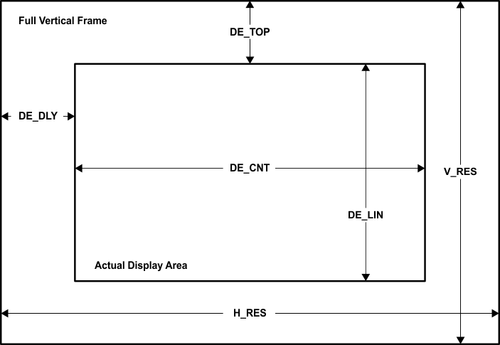
The TFP410 contains a DE generator that can be used to generate an internal DE signal when the original data source does not provide one. There are several I2C programmable values that control the DE generator (see Figure 6-4). DE_GEN in the DE_CTL register enables this function. When enabled, the DE pin is ignored.
DE_TOP and DE_LIN are line counts used to control the number of lines after VSYNC goes active that DE is enabled, and the total number of lines that DE remains active, respectively. The polarity of VSYNC must be set by VS_POL in the DE_CTL register.
DE_DLY and DE_CNT are pixel counts used to control the number of pixels after HSYNC goes active that DE is enabled, and the total number of pixels that DE remains active, respectively. The polarity of HSYNC must be set by HS_POL in the DE_CTL register.
The TFP410 also counts the total number of HSYNC pulses between VSYNC pulses, and the total number of pixels between HSYNC pulses. These values, the total vertical and horizontal resolutions, are available in V_RES and H_RES, respectively. These values are available at all times, whether or not the DE generator is enabled.
 Figure 6-4 DE
Generator Register Functions