SLOS382E September 2001 – May 2015 THS3122 , THS3125
PRODUCTION DATA.
- 1 Features
- 2 Applications
- 3 Description
- 4 Revision History
- 5 Device Options
- 6 Pin Configuration and Functions
-
7 Specifications
- 7.1 Absolute Maximum Ratings
- 7.2 Dissipation Ratings Table
- 7.3 Recommended Operating Conditions
- 7.4 Electrical Characteristics: Dynamic Performance
- 7.5 Electrical Characteristics: Noise and Distortion Performance
- 7.6 Electrical Characteristics: DC Performance
- 7.7 Electrical Characteristics: Input Characteristics
- 7.8 Electrical Characteristics: Output Characteristics
- 7.9 Electrical Characteristics: Power Supply
- 7.10 Electrical Characteristics: Shutdown Characteristics (THS3125 Only)
- 7.11 Typical Characteristics: Table Of Graphs
- 7.12 Typical Characteristics
- 8 Detailed Description
- 9 Application and Implementation
- 10Layout
- 11Device and Documentation Support
- 12Mechanical, Packaging, and Orderable Information
パッケージ・オプション
メカニカル・データ(パッケージ|ピン)
サーマルパッド・メカニカル・データ
- PWP|14
発注情報
6 Pin Configuration and Functions
THS3122: D and DDA Packages
SOIC-8 and HSOP-8
Top View

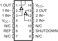
THS3125: D and PWP Packages
SOIC-14 and HTSSOP-14
Top View

Pin Functions
| PIN | I/O | DESCRIPTION | ||
|---|---|---|---|---|
| NAME | THS3122 | THS3125 | ||
| 1 IN+ | 3 | 3 | I | Noninverting amplifier 1 input |
| 1 IN– | 2 | 2 | I | Inverting amplifier 1 input |
| 1 OUT | 1 | 1 | O | Amplifier 1 output |
| 2 IN+ | 5 | 11 | I | Noninverting amplifier 2 input |
| 2 IN– | 6 | 12 | I | Inverting amplifier 2 input |
| 2 OUT | 7 | 13 | O | Amplifier 2 output |
| N/C | — | 5, 7, 8, 10 | — | No internal connection. |
| SHUTDOWN | — | 9 | I | Shutdown control. Logic low = active; logic high = power down. |
| REF | — | 6 | I | Reference for shutdown threshold control |
| VCC+ | 8 | 14 | P | Positive power supply |
| VCC– | 4 | 4 | P | Negative power supply |