JAJSMD3L April   2000  – August 2023 THS4130 , THS4131

PRODUCTION DATA  

  1.   1
  2. 特長
  3. アプリケーション
  4. 概要
  5. Revision History
  6. Device Comparison Table
  7. Pin Configuration and Functions
  8. Specifications
    1. 7.1 Absolute Maximum Ratings
    2. 7.2 ESD Ratings
    3. 7.3 Recommended Operating Conditions
    4. 7.4 Thermal Information
    5. 7.5 Electrical Characteristics
    6. 7.6 Typical Characteristics
  9. Detailed Description
    1. 8.1 Overview
    2. 8.2 Functional Block Diagram
    3. 8.3 Feature Description
    4. 8.4 Device Functional Modes
      1. 8.4.1 Power-Down Mode
  10. Application and Implementation
    1. 9.1 Application Information
      1. 9.1.1 Output Common-Mode Voltage
        1. 9.1.1.1 Resistor Matching
      2. 9.1.2 Driving a Capacitive Load
      3. 9.1.3 Data Converters
      4. 9.1.4 Single-Supply Applications
    2. 9.2 Typical Application
      1. 9.2.1 Design Requirements
      2. 9.2.2 Detailed Design Procedure
      3. 9.2.3 Application Curve
    3. 9.3 Power Supply Recommendations
    4. 9.4 Layout
      1. 9.4.1 Layout Guidelines
        1. 9.4.1.1 PowerPAD™ Integrated Circuit Package Design Considerations
      2. 9.4.2 Layout Example
  11. 10Device and Documentation Support
    1. 10.1 Documentation Support
      1. 10.1.1 Related Documentation
    2. 10.2 ドキュメントの更新通知を受け取る方法
    3. 10.3 サポート・リソース
    4. 10.4 Trademarks
    5. 10.5 静電気放電に関する注意事項
    6. 10.6 用語集
  12. 11Mechanical, Packaging, and Orderable Information

パッケージ・オプション

メカニカル・データ(パッケージ|ピン)
サーマルパッド・メカニカル・データ
発注情報

Typical Application

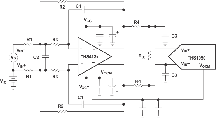
GUID-296BC887-8B09-4237-BC68-F4C9A8F72241-low.gif Figure 9-5 Antialias Filtering

For signal conditioning in ADC applications, make sure to limit the input frequency to the ADC. Low-pass filters can prevent the aliasing of the high-frequency noise with the frequency of operation. This design example shows a method by which the noise can be filtered in the THS413x. Figure 9-5 shows the design example for the THS413x in active low-pass filter topology driving an ADC.