SLOS547A November 2008 – November 2015 THS4509-Q1
PRODUCTION DATA.
- 1 Features
- 2 Applications
- 3 Description
- 4 Revision History
- 5 Pin Configuration and Functions
- 6 Specifications
- 7 Detailed Description
-
8 Application and Implementation
- 8.1 Application Information
- 8.2 Typical Applications
- 9 Power Supply Recommendations
- 10Layout
- 11Device and Documentation Support
- 12Mechanical, Packaging, and Orderable Information
パッケージ・オプション
メカニカル・データ(パッケージ|ピン)
- RGT|16
サーマルパッド・メカニカル・データ
- RGT|16
発注情報
8 Application and Implementation
NOTE
Information in the following applications sections is not part of the TI component specification, and TI does not warrant its accuracy or completeness. TI’s customers are responsible for determining suitability of components for their purposes. Customers should validate and test their design implementation to confirm system functionality.
8.1 Application Information
The following circuits show application information for the THS4509-Q1. For simplicity, power supply decoupling capacitors are not shown in these diagrams. See THS4509-Q1 EVM for recommendations. For more detail on the use and operation of fully differential op amps see the application report Fully-Differential Amplifiers (SLOA054) .
8.1.1 Test Circuits
The THS4509-Q1 is tested with the following test circuits built on the EVM. For simplicity, power-supply decoupling is not shown – see layout in the applications section for recommendations. Depending on the test conditions, component values are changed per the following tables, or as otherwise noted. The signal generators used are ac coupled 50-Ω sources and a 0.22-μF capacitor and a 49.9-Ω resistor to ground are inserted across RIT on the alternate input to balance the circuit. A split power supply is used to ease the interface to common test equipment, but the amplifier can be operated single supply, as described in the applications section, with no impact on performance.
Table 3. Gain Component Values
| GAIN | RF | RG | RIT |
|---|---|---|---|
| 6 dB | 348 Ω | 165 Ω | 61.9 Ω |
| 10 dB | 348 Ω | 100 Ω | 69.8 Ω |
| 14 dB | 348 Ω | 56.2 Ω | 88.7 Ω |
| 20 dB | 348 Ω | 16.5 Ω | 287 Ω |
SPACE
NOTE
The gain setting includes 50-Ω source impedance. Components are chosen to achieve gain and 50-Ω input termination.
Table 4. Load Component Values
| RL | RO | ROT | ATTEN |
|---|---|---|---|
| 100 Ω | 25 Ω | open | 6 dB |
| 200 Ω | 86.6 Ω | 69.8 Ω | 16.8 dB |
| 499 Ω | 237 Ω | 56.2 Ω | 25.5 dB |
| 1k Ω | 487 Ω | 52.3 Ω | 31.8 dB |
SPACE
NOTE
Note the total load includes 50-Ω termination by the test equipment. Components are chosen to achieve load and 50-Ω line termination through a 1:1 transformer.
Due to the voltage divider on the output formed by the load component values, the amplifier's output is attenuated. The column ATTEN in Table 4 shows the attenuation expected from the resistor divider. When using a transformer at the output, as shown in Figure 77, the signal sees slightly more loss, and these numbers are approximate.
8.1.1.1 Frequency Response
The circuit shown in Figure 76 is used to measure the frequency response of the circuit.
A network analyzer is used as the signal source and as the measurement device. The output impedance of the network analyzer is 50 Ω. RIT and RG are chosen to impedance match to 50 Ω, and to maintain the proper gain. To balance the amplifier, a 0.22-µF capacitor and 49.9-Ω resistor to ground are inserted across RIT on the alternate input.
The output is probed using a high-impedance differential probe across the 100-Ω resistor. The gain is referred to the amplifier output by adding back the 6-dB loss due to the voltage divider on the output.
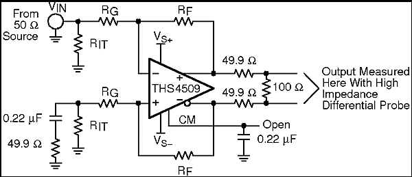 Figure 76. Frequency Response Test Circuit
8.1.1.2 Distortion and 1-dB Compression
The circuit shown in Figure 77 is used to measure harmonic distortion, intermodulation distortion, and 1-db compression point of the amplifier.
A signal generator is used as the signal source and the output is measured with a spectrum analyzer. The output impedance of the signal generator is 50 Ω. RIT and RG are chosen to impedance-match to 50 Ω, and to maintain the proper gain. To balance the amplifier, a 0.22-µF capacitor and 49.9-Ω resistor to ground are inserted across RIT on the alternate input.
A low-pass filter is inserted in series with the input to reduce harmonics generated at the signal source. The level of the fundamental is measured, then a high-pass filter is inserted at the output to reduce the fundamental so that it does not generate distortion in the input of the spectrum analyzer.
The transformer used in the output to convert the signal from differential to single ended is an ADT1-1WT. It limits the frequency response of the circuit so that measurements cannot be made below approximately 1 MHz.
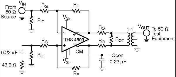 Figure 77. Distortion Test Circuit
The 1-dB compression point is measured with a spectrum analyzer with 50-Ω double termination or 100-Ω termination as shown in Table 4. The input power is increased until the output is 1 dB lower than expected. The number reported in the table data is the power delivered to the spectrum analyzer input. Add 3 dB to see the amplifier output.
8.1.1.3 S-Parameter, Slew Rate, Transient Response, Settling Time, Output Impedance, Overdrive, Output Voltage, and Turn-On and Turn-Off Time
The circuit shown in Figure 78 is used to measure s-parameters, slew rate, transient response, settling time, output impedance, overdrive recovery, output voltage swing, and turnon and turnoff times of the amplifier. For output impedance, the signal is injected at VOUT with VIN left open and the drop across the 49.9-Ω resistor is used to calculate the impedance seen looking into the amplifier’s output.
Because S21 is measured single ended at the load with 50-Ω double termination, add 12 dB to refer to the amplifier’s output as a differential signal.
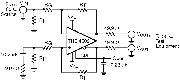 Figure 78. S-Parameter, Sr, Transient Response, Settling Time, ZO, Overdrive Recovery, VOUT Swing, and Turnon and Turnoff Test Circuit
8.1.1.4 CM Input
The circuit shown in Figure 79 is used to measure the frequency response and input impedance of the CM input. Frequency response is measured single ended at VOUT+ or VOUT– with the input injected at VIN, RCM = 0 Ω, and RCMT = 49.9 Ω. The input impedance is measured with RCM = 49.9 Ω with RCMT = open, and calculated by measuring the voltage drop across RCM to determine the input current.
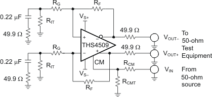 Figure 79. CM Input Test Circuit
8.1.1.5 CMRR and PSRR
The circuit shown in Figure 80 is used to measure the CMRR and PSRR of VS+ and VS–. The input is switched appropriately to match the test being performed.
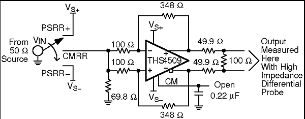 Figure 80. CMRR and PSRR Test Circuit
8.1.2 Differential Input to Differential Output Amplifier
The THS4509-Q1 is a fully differential op amp, and can be used to amplify differential input signals to differential output signals. A basic block diagram of the circuit is shown in Figure 81 (CM input not shown). The gain of the circuit is set by RF divided by RG.
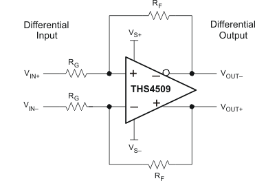 Figure 81. Differential Input to Differential Output Amplifier
Depending on the source and load, input and output termination can be accomplished by adding RIT and RO.
8.1.3 Single-Ended Input to Differential Output Amplifier
The THS4509-Q1 can be used to amplify and convert single-ended input signals to differential output signals. A basic block diagram of the circuit is shown in Figure 82 (CM input not shown). The gain of the circuit is again set by RF divided by RG.
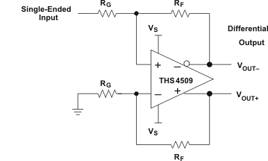 Figure 82. Single-Ended Input to Differential Output Amplifier
8.1.4 Input Common-Mode Voltage Range
The input common-model voltage of a fully differential op amp is the voltage at the + and – input pins of the op amp.
It is important to not violate the input common-mode voltage range (VICR) of the op amp. Assuming the op amp is in linear operation the voltage across the input pins is only a few millivolts at most. So finding the voltage at one input pin will determine the input common-mode voltage of the op amp.
Treating the negative input as a summing node, the voltage is given by Equation 1:

To determine the VICR of the op amp, the voltage at the negative input is evaluated at the extremes of VOUT+.
As the gain of the op amp increases, the input common-mode voltage becomes closer and closer to the input common-mode voltage of the source.
8.1.5 Setting the Output Common-Mode Voltage
The output common-mode voltage is set by the voltage at the CM pin(s). The internal common-mode control circuit maintains the output common-mode voltage within 3-mV offset (typical) from the set voltage, when set within 0.5 V of mid-supply, with less than 4-mV differential offset voltage. If left unconnected, the common-mode set point is set to mid-supply by internal circuitry, which may be overdriven from an external source. Figure 83 is representative of the CM input. The internal CM circuit has about 700 MHz of –3-dB bandwidth, which is required for best performance, but it is intended to be a DC bias input pin. To reduce noise at the output, TI recommends bypass capacitors are recommended on this pin. The external current required to overdrive the internal resistor divider is given by Equation 2:

where
- VCM is the voltage applied to the CM pin.
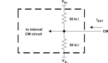 Figure 83. CM Input Circuit
8.1.6 Single-Supply Operation (3 V to 5 V)
To facilitate testing with common lab equipment, the THS4509-Q1 EVM allows split-supply operation, and the characterization data presented in this data sheet was taken with split-supply power inputs. The device can easily be used with a single-supply power input without degrading the performance. Figure 84, Figure 85, and Figure 86 show DC and AC-coupled single-supply circuits with single-ended inputs. These configurations all allow the input and output common-mode voltage to be set to mid-supply allowing for optimum performance. The information presented here can also be applied to differential input sources.
In Figure 84, the source is referenced to the same voltage as the CM pin (VCM). VCM is set by the internal circuit to mid-supply. RT along with the input impedance of the amplifier circuit provides input termination, which is also referenced to VCM.
Note RS and RT are added to the alternate input from the signal input to balance the amplifier. Alternately, one resistor can be used equal to the combined value RG+ RS||RT on this input. This is also true of the circuits shown in Figure 85 and Figure 86.
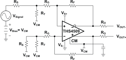 Figure 84. THS4509-Q1 DC-Coupled Single Supply With Input Biased to VCM
In Figure 85 the source is referenced to ground and so is the input termination resistor. RPU is added to the circuit to avoid violating the VICR of the op amp. The proper value of resistor to add can be calculated from Equation 3:

where
- VIC is the desire input common-mode voltage
- VCM = CM
- RIN = RG + RS||RT
To set to mid-supply, make the value of RPU = RG+ RS||RT.
Table 5 is a modification of Table 3 to add the proper values with RPU assuming a 50-Ω source impedance and setting the input and output common-mode voltage to mid-supply.
There are two drawbacks to this configuration. One is it requires additional current from the power supply. Using the values shown for a gain of 10 dB requires 37 mA more current with 5-V supply, and 22 mA more current with 3-V supply.
The other drawback is this configuration also increases the noise gain of the circuit. In the 10-dB gain case, noise gain increases by a factor of 1.5.
Table 5. RPU Values for Various Gains
| GAIN | RF | RG | RIT | RPU |
|---|---|---|---|---|
| 6 dB | 348 Ω | 169 Ω | 64.9 Ω | 200 Ω |
| 10 dB | 348 Ω | 102 Ω | 78.7 Ω | 133 Ω |
| 14 dB | 348 Ω | 61.9 Ω | 115 Ω | 97.6 Ω |
| 20 dB | 348 Ω | 40.2 Ω | 221 Ω | 80.6 Ω |
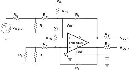 Figure 85. THS4509-Q1 DC-Coupled Single Supply With RPU Used to Set VIC
Figure 86 shows AC coupling to the source. Using capacitors in series with the termination resistors allows the amplifier to self bias both input and output to mid-supply.
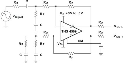 Figure 86. THS4509-Q1 AC-Coupled Single Supply
8.2 Typical Applications
8.2.1 THS4509-Q1 + ADS5500-EP Combined Performance
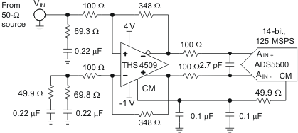 Figure 87. THS4509-Q1 + ADS5500-EP Circuit
8.2.1.1 Design Requirements
The THS4509-Q1 can be used in adjacent applications, such as industrial, in combination with HiRel devices. As automotive standards are similar to industrial standards, automotive devices are often suitable alternative options for the industrial customers. Applications using fully differential amplifiers have several requirements. The main requirements are high linearity and good signal amplitude. Linearity is accomplished by using well matched feedback and gain set resistors as well as an appropriate supply voltage. The signal amplitude can be tailored by using an appropriate gain. In this design the gain is set for a gain of 3.48 (RF=348/ RG=100), the SFDR is 80 dBc, and the SNR is 69 dBc at a frequency of 70 Mhz. The supply voltages are set to 4 V and –1 V and the output common mode is 1.55 V. The TSH4509 can be placed into shutdown to reduce power dissipation to less than 5 mW.
8.2.1.2 Detailed Design Procedure
The THS4509-Q1 is designed to be a high performance drive amplifier for high performance data converters like the ADS5500-EP 14-bit 125-MSPS ADC. Figure 87 shows a circuit combining the two devices, and Figure 88 shows the combined SNR and SFDR performance versus frequency with –1-dBFS input signal level sampling at 125 MSPS. The THS4509-Q1 amplifier circuit provides 10 dB of gain, converts the single-ended input to differential, and sets the proper input common-mode voltage to the ADS5500-EP. The 100-Ω resistors and 2.7-pF capacitor between the THS4509-Q1 outputs and ADS5500-EP inputs along with the input capacitance of the ADS5500-EP limit the bandwidth of the signal to 115 MHz (–3 dB). For testing, a signal generator is used for the signal source. The generator is an AC-coupled 50-Ω source. A band-pass filter is inserted in series with the input to reduce harmonics and noise from the signal source. Input termination is accomplished via the 69.8-Ω resistor and 0.22-µF capacitor to ground in conjunction with the input impedance of the amplifier circuit. A 0.22-µF capacitor and 49.9-Ω resistor are inserted to ground across the 69.8-Ω resistor and 0.22-µF capacitor on the alternate input to balance the circuit. Gain is a function of the source impedance, termination, and 348-Ω feedback resistor. See Table 5 for component values to set proper 50-Ω termination for other common gains. A split power supply of 4 V and –1 V is used to set the input and output common-mode voltages to approximately mid-supply while setting the input common-mode of the ADS5500-EP to the recommended 1.55 V. This maintains maximum headroom on the internal transistors of the THS4509-Q1 to ensure optimum performance.
Figure 89 shows the two-tone FFT of the THS4509-Q1 + ADS5500-EP circuit with 65-MHz and 70-MHz input frequencies. The SFDR is 90 dBc.
8.2.1.3 Application Curves
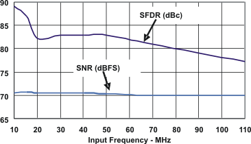
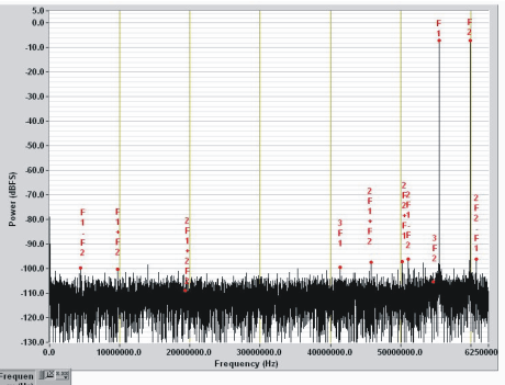 Figure 89. THS4509-Q1 + ADS5500-EP Two-Tone Fft With 65-MHz and 70-MHz Input
8.2.2 THS4509-Q1 + ADS5424-SP Combined Performance
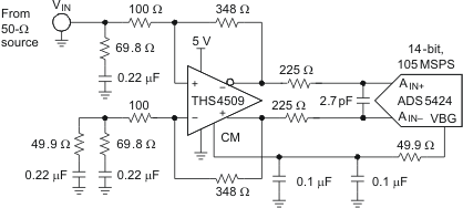 Figure 90. THS4509-Q1 + ADS5424-SP Circuit
8.2.2.1 Detailed Design Procedure
Figure 90 shows the THS4509-Q1 driving the ADS5424-SP ADC, and Figure 91 shows their combined SNR and SFDR performance versus frequency with –1-dBFS input signal level and sampling at 80 MSPS.
As before, the THS4509-Q1 amplifier provides 10 dB of gain, converts the single-ended input to differential, and sets the proper input common-mode voltage to the ADS5424-SP. Input termination and circuit testing is the same as previously described for the THS4509-Q1 + ADS5500-EP circuit.
The 225-Ω resistors and 2.7-pF capacitor between the THS4509-Q1 outputs and ADS5424-SP inputs (along with the input capacitance of the ADC) limit the bandwidth of the signal to about 100 MHz (–3 dB).
Since the ADS5424-SP's recommended input common-mode voltage is 2.4 V, the THS4509-Q1 is operated from a single power-supply input with VS+ = 5 V and VS– = 0 V (ground).
8.2.2.2 Application Curve
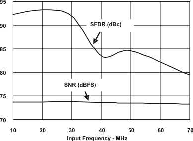 Figure 91. THS4509-Q1 + ADS5424-SP SFDR and SNR Performance vs Frequency