SLOS547A November 2008 – November 2015 THS4509-Q1
PRODUCTION DATA.
- 1 Features
- 2 Applications
- 3 Description
- 4 Revision History
- 5 Pin Configuration and Functions
- 6 Specifications
- 7 Detailed Description
-
8 Application and Implementation
- 8.1 Application Information
- 8.2 Typical Applications
- 9 Power Supply Recommendations
- 10Layout
- 11Device and Documentation Support
- 12Mechanical, Packaging, and Orderable Information
パッケージ・オプション
メカニカル・データ(パッケージ|ピン)
- RGT|16
サーマルパッド・メカニカル・データ
- RGT|16
発注情報
7 Detailed Description
7.1 Overview
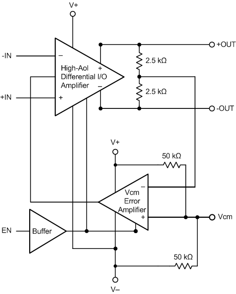
The THS4509-Q1 is a fully differential amplifier designed to provide low distortion amplification to wide bandwidth differential signals. The THS4509-Q1, though fully integrated for ultimate balance and distortion performance, functionally provides three channels. Two of these channels are the positive and negative signal path channels, which function similarly to inverting mode operational amplifiers and are the primary signal paths. The third channel is the common-mode feedback circuit. This is the circuit that sets the output common mode as well as driving the positive and negative outputs to be equal magnitude and opposite phase, even when only one of the two input channels is driven. The common-mode feedback circuit allows single-ended to differential operation.
7.2 Functional Block Diagram

7.3 Feature Description
THS4509-Q1 fully differential amplifier requires external resistors to set a minimum gain of 6 db and optimized gain of 10 db for correct signal-path operation. When configured for the desired input impedance and gain setting with these external resistors, the amplifier can be either on with the PD pin asserted to a voltage greater than Vs– + 2.1 V, or turned off by asserting PD low. Disabling the amplifier shuts off the quiescent current and stops correct amplifier operation. The signal path is still present for the source signal through the external resistors. The CM control pin sets the output average voltage. Left open, CM voltage defaults to an internal midsupply value. Driving the CM input with a voltage reference within its valid range sets a target for the internal common mode error amplifier.
7.4 Device Functional Modes
An integrated, fully-differential amplifier is very similar in architecture to a standard, voltage feedback operational amplifier, with a few differences. Both types of amplifiers have differential inputs. Fully differential amplifiers have differential outputs, while a standard operational amplifier’s output is single-ended. In a fully-differential amplifier, the output is differential and the output common-mode voltage can be controlled independently of the differential voltage. The purpose of the Vocm input in the fully-differential amplifier is to set the output common-mode voltage. Vocm is biased to the midpoint between positive and negative supplies by an internal voltage divider In a standard operational amplifier with single-ended output, the output common-mode voltage and the signal are the same thing. There is typically one feedback path from the output to the negative input in a standard operational amplifier. A fully-differential amplifier has multiple feedback paths.