SBOS458H December 2008 – June 2015 THS4521 , THS4522 , THS4524
PRODUCTION DATA.
- 1 Features
- 2 Applications
- 3 Description
- 4 Revision History
- 5 Device Comparison Table
- 6 Pin Configuration and Functions
-
7 Specifications
- 7.1 Absolute Maximum Ratings
- 7.2 ESD Ratings
- 7.3 Recommended Operating Conditions
- 7.4 Thermal Information
- 7.5 Electrical Characteristics: VS+ - VS- = 3.3 V
- 7.6 Electrical Characteristics: VS+ - VS- = 5 V
- 7.7 Typical Characteristics
- 7.8 Typical Characteristics: VS+ - VS- = 3.3 V
- 7.9 Typical Characteristics: 5 V
-
8 Detailed Description
- 8.1 Overview
- 8.2 Functional Block Diagram
- 8.3
Feature Description
- 8.3.1 Frequency Response
- 8.3.2 Distortion
- 8.3.3 Slew Rate, Transient Response, Settling Time, Output Impedance, Overdrive, Output Voltage, and Turn-On/Turn-Off Time
- 8.3.4 Common-Mode and Power-Supply Rejection
- 8.3.5 VOCM Input
- 8.3.6 Typical Performance Variation With Supply VoltageTypical Performance Variation with Supply Voltage section
- 8.3.7 title of Single-Supply Operation sectionSingle-Supply Operation
- 8.3.8 Low-Power Applications and the Effects of Resistor Values on Bandwidth
- 8.3.9 Frequency Response Variation due to Package Options
- 8.3.10 Driving Capacitive Loads
- 8.3.11 Audio Performance
- 8.3.12 Audio On/Off Pop Performance
- 8.4
Device Functional Modes
- 8.4.1
Operation from Single-Ended Sources to Differential Outputs
- 8.4.1.1 AC-Coupled Signal Path Considerations for Single-Ended Input to Differential Output Conversion
- 8.4.1.2 DC-Coupled Input Signal Path Considerations for Single-Ended to Differential Conversion
- 8.4.1.3 Resistor Design Equations for the Single-Ended to Differential Configuration of the FDA
- 8.4.1.4 Input Impedance for the Single-Ended to Differential FDA Configuration
- 8.4.2 Differential-Input to Differential-Output Operation
- 8.4.1
Operation from Single-Ended Sources to Differential Outputs
- 8.5 Programming
-
9 Application and Implementation
- 9.1 Application Information
- 9.2 Typical Applications
- 10Power Supply Recommendations
- 11Layout
- 12Device and Documentation Support
- 13Mechanical, Packaging, and Orderable Information
パッケージ・オプション
メカニカル・データ(パッケージ|ピン)
サーマルパッド・メカニカル・データ
発注情報
6 Pin Configuration and Functions
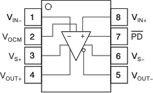
THS4521 D and DGK Package
8-Pin SOIC and VSSOP
Top View

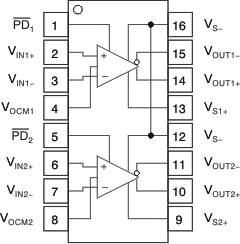
THS4522 PW Package
16-Pin TSSOP
Top View

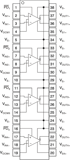
THS4524 DBT Package
38-Pin TSSOP
Top View

Pin Functions: THS4521
| PIN | DESCRIPTION | |
|---|---|---|
| NAME | NO. | |
| VIN– | 1 | Inverting amplifier input |
| VOCM | 2 | Common-mode voltage input |
| VS+ | 3 | Amplifier positive power-supply input |
| VOUT+ | 4 | Noninverting amplifier output |
| VOUT– | 5 | Inverting amplifier output |
| VS– | 6 | Amplifier negative power-supply input. Note that VS– is tied together on multi-channel devices. |
| PD | 7 | Power down. PD = logic low puts device into low-power mode. PD = logic high or open for normal operation. |
| VIN+ | 8 | Noninverting amplifier input |
Pin Functions: THS4522
| PIN | DESCRIPTION | |
|---|---|---|
| NAME | NO. | |
| PD1 | 1 | Power down 1. PD = logic low puts device into low-power mode. PD = logic high or open for normal operation. |
| VIN1+ | 2 | Noninverting amplifier 1 input |
| VIN1– | 3 | Inverting amplifier 1 input |
| VOCM1 | 4 | Common-mode voltage input 1 |
| PD2 | 5 | Power down 2. PD = logic low puts device into low-power mode. PD = logic high or open for normal operation. |
| VIN2+ | 6 | Noninverting amplifier 2 input |
| VIN2– | 7 | Inverting amplifier 2 input |
| VOCM2 | 8 | Common-mode voltage input 2 |
| VS+2 | 9 | Amplifier 2 positive power-supply input |
| VOUT2+ | 10 | Noninverting amplifier 2 output |
| VOUT2– | 11 | Inverting amplifier 2 output |
| VS– | 12 | Negative power-supply input. Note that VS– is tied together on multi-channel devices. |
| VS+1 | 13 | Amplifier 1 positive power-supply input |
| VOUT1+ | 14 | Noninverting amplifier 1 output |
| VOUT1– | 15 | Inverting amplifier 1 output |
| VS– | 16 | Negative power-supply input. Note that VS– is tied together on multi-channel devices. |
Pin Functions: THS4524
| PIN | DESCRIPTION | |
|---|---|---|
| NAME | NO. | |
| PD1 | 1 | Power down 1. PD = logic low puts channel into low-power mode. PD = logic high or open for normal operation. |
| VIN1+ | 2 | Noninverting amplifier 1 input |
| VIN1– | 3 | Inverting amplifier 1 input |
| VOCM1 | 4 | Common-mode voltage input 1 |
| VS– | 5 | Negative power-supply input. Note that VS– is tied together on multi-channel devices. |
| PD2 | 6 | Power down 2. PD = logic low puts channel into low-power mode. PD = logic high or open for normal operation. |
| VIN2+ | 7 | Noninverting amplifier 2 input |
| VIN2– | 8 | Inverting amplifier 2 input |
| VOCM2 | 9 | Common-mode voltage input 2 |
| VS– | 10 | Negative power-supply input. Note that VS– is tied together on multi-channel devices. |
| PD3 | 11 | Power down 3. PD = logic low puts channel into low-power mode. PD = logic high or open for normal operation. |
| VIN3+ | 12 | Noninverting amplifier 3 input |
| VIN3– | 13 | Inverting amplifier 3 input |
| VOCM3 | 14 | Common-mode voltage input 3 |
| VS– | 15 | Negative power-supply input. Note that VS– is tied together on multi-channel devices. |
| PD4 | 16 | Power down 4. PD = logic low puts channel into low-power mode. PD = logic high or open for normal operation. |
| VIN4+ | 17 | Noninverting amplifier 4 input |
| VIN4– | 18 | Inverting amplifier 4 input |
| VOCM4 | 19 | Common-mode voltage input 4 |
| VS4+ | 20 | Amplifier 4 positive power-supply input |
| VOUT4+ | 21 | Noninverting amplifier 4 output |
| VOUT4– | 22 | Inverting amplifier 4 output |
| VS– | 23 | Negative power-supply input. Note that VS– is tied together on multi-channel devices. |
| VS– | 24 | Negative power-supply input. Note that VS– is tied together on multi-channel devices. |
| VS3+ | 25 | Amplifier 3 positive power-supply input |
| VOUT3+ | 26 | Noninverting amplifier3 output |
| VOUT3– | 27 | Inverting amplifier3 output |
| VS– | 28 | Negative power-supply input. Note that VS– is tied together on multi-channel devices. |
| VS– | 29 | Negative power-supply input. Note that VS– is tied together on multi-channel devices. |
| VS2+ | 30 | Amplifier 2 positive power-supply input |
| VOUT2+ | 31 | Noninverting amplifier 2 output |
| VOUT2– | 32 | Inverting amplifier 2 output |
| VS– | 33 | Negative power-supply input. Note that VS– is tied together on multi-channel devices. |
| VS– | 34 | Negative power-supply input. Note that VS– is tied together on multi-channel devices. |
| VS1+ | 35 | Amplifier 1 positive power-supply input |
| VOUT1+ | 36 | Noninverting amplifier 1 output |
| VOUT1– | 37 | Inverting amplifier 1 output |
| VS– | 38 | Negative power-supply input. Note that VS– is tied together on multi-channel devices. |