SBOS458H December 2008 – June 2015 THS4521 , THS4522 , THS4524
PRODUCTION DATA.
- 1 Features
- 2 Applications
- 3 Description
- 4 Revision History
- 5 Device Comparison Table
- 6 Pin Configuration and Functions
-
7 Specifications
- 7.1 Absolute Maximum Ratings
- 7.2 ESD Ratings
- 7.3 Recommended Operating Conditions
- 7.4 Thermal Information
- 7.5 Electrical Characteristics: VS+ - VS- = 3.3 V
- 7.6 Electrical Characteristics: VS+ - VS- = 5 V
- 7.7 Typical Characteristics
- 7.8 Typical Characteristics: VS+ - VS- = 3.3 V
- 7.9 Typical Characteristics: 5 V
-
8 Detailed Description
- 8.1 Overview
- 8.2 Functional Block Diagram
- 8.3
Feature Description
- 8.3.1 Frequency Response
- 8.3.2 Distortion
- 8.3.3 Slew Rate, Transient Response, Settling Time, Output Impedance, Overdrive, Output Voltage, and Turn-On/Turn-Off Time
- 8.3.4 Common-Mode and Power-Supply Rejection
- 8.3.5 VOCM Input
- 8.3.6 Typical Performance Variation With Supply VoltageTypical Performance Variation with Supply Voltage section
- 8.3.7 title of Single-Supply Operation sectionSingle-Supply Operation
- 8.3.8 Low-Power Applications and the Effects of Resistor Values on Bandwidth
- 8.3.9 Frequency Response Variation due to Package Options
- 8.3.10 Driving Capacitive Loads
- 8.3.11 Audio Performance
- 8.3.12 Audio On/Off Pop Performance
- 8.4
Device Functional Modes
- 8.4.1
Operation from Single-Ended Sources to Differential Outputs
- 8.4.1.1 AC-Coupled Signal Path Considerations for Single-Ended Input to Differential Output Conversion
- 8.4.1.2 DC-Coupled Input Signal Path Considerations for Single-Ended to Differential Conversion
- 8.4.1.3 Resistor Design Equations for the Single-Ended to Differential Configuration of the FDA
- 8.4.1.4 Input Impedance for the Single-Ended to Differential FDA Configuration
- 8.4.2 Differential-Input to Differential-Output Operation
- 8.4.1
Operation from Single-Ended Sources to Differential Outputs
- 8.5 Programming
-
9 Application and Implementation
- 9.1 Application Information
- 9.2 Typical Applications
- 10Power Supply Recommendations
- 11Layout
- 12Device and Documentation Support
- 13Mechanical, Packaging, and Orderable Information
8 Detailed Description
8.1 Overview
The THS4521, THS4522, and THS4524 family is tested with the test circuits shown in this section; all circuits are built using the available THS4521 evaluation module (EVM). For simplicity, power-supply decoupling is not shown; see the layout in the Typical Applications section for recommendations. Depending on the test conditions, component values change in accordance with Table 4 and Table 5, or as otherwise noted. In some cases the signal generators used are ac-coupled and in others they dc-coupled 50-Ω sources. To balance the amplifier when ac-coupled, a 0.22-μF capacitor and 49.9-Ω resistor to ground are inserted across RIT on the alternate input; when dc-coupled, only the 49.9-Ω resistor to ground is added across RIT. A split power supply is used to ease the interface to common test equipment, but the amplifier can be operated in a single-supply configuration as described in the Typical Applications section with no impact on performance. Also, for most of the tests, except as noted, the devices are tested with single-ended inputs and a transformer on the output to convert the differential output to single-ended because common lab test equipment has single-ended inputs and outputs. Similar or better performance can be expected with differential inputs and outputs.
As a result of the voltage divider on the output formed by the load component values, the amplifier output is attenuated. The Atten column in Table 5 shows the attenuation expected from the resistor divider. When using a transformer at the output (as shown in Figure 55), the signal sees slightly more loss because of transformer and line loss; these numbers are approximate.
Table 4. Gain Component Values for Single-Ended Input (see Figure 54)
| Gain | RF | RG | RIT |
|---|---|---|---|
| 1 V/V | 1 kΩ | 1 kΩ | 52.3 Ω |
| 2 V/V | 1 kΩ | 487 Ω | 53.6 Ω |
| 5 V/V | 1 kΩ | 191 Ω | 59.0 Ω |
| 10 V/V | 1 kΩ | 86.6 Ω | 69.8 Ω |
- Gain setting includes 50-Ω source impedance. Components are chosen to achieve gain and 50-Ω input termination.
Table 5. Load Component Values For 1:1 Differential To Single-Ended Output Transformer (See Figure 55)
| RL | RO | ROT | Atten |
|---|---|---|---|
| 100 Ω | 24.9 Ω | Open | 6 dB |
| 200 Ω | 86.6 Ω | 69.8 Ω | 16.8 dB |
| 499 Ω | 237 Ω | 56.2 Ω | 25.5 dB |
| 1 kΩ | 487 Ω | 52.3 Ω | 31.8 dB |
- Total load includes 50-Ω termination by the test equipment. Components are chosen to achieve load and 50-Ω line termination through a 1:1 transformer.
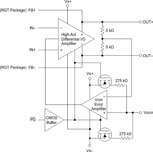
8.2 Functional Block Diagram
8.3 Feature Description
8.3.1 Frequency Response
The circuit shown in Figure 54 is used to measure the frequency response of the circuit.
A network analyzer is used as the signal source and the measurement device. The output impedance of the network analyzer is dc-coupled and is 50 Ω. RIT and RG are chosen to impedance-match to 50 Ω and maintain the proper gain. To balance the amplifier, a 49.9-Ω resistor to ground is inserted across RIT on the alternate input.
The output is probed using a Tektronix high-impedance differential probe across the 953-Ω resistor and referred to the amplifier output by adding back the 0.42-dB because of the voltage divider on the output.
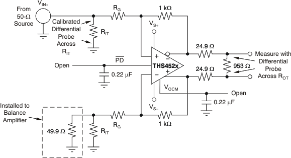 Figure 54. Frequency Response Test Circuit
8.3.2 Distortion
The circuit shown in Figure 55 is used to measure harmonic and intermodulation distortion of the amplifier.
A signal generator is used as the signal source and the output is measured with a Rhode and Schwarz spectrum analyzer. The output impedance of the HP signal generator is ac-coupled and is 50 Ω. RIT and RG are chosen to impedance match to 50 Ω and maintain the proper gain. To balance the amplifier, a 0.22-μF capacitor and 49.9-Ω resistor to ground are inserted across RIT on the alternate input.
A low-pass filter is inserted in series with the input to reduce harmonics generated at the signal source. The level of the fundamental is measured and then a notch filter is inserted at the output to reduce the fundamental so it does not generate distortion in the input of the spectrum analyzer.
The transformer used in the output to convert the signal from differential to single-ended is an ADT1–1WT. It limits the frequency response of the circuit so that measurements cannot be made below approximately 1 MHz.
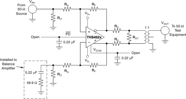 Figure 55. Distortion Test Circuit
8.3.3 Slew Rate, Transient Response, Settling Time, Output Impedance, Overdrive, Output Voltage, and Turn-On/Turn-Off Time
The circuit shown in Figure 56 is used to measure slew rate, transient response, settling time, output impedance, overdrive recovery, output voltage swing, and ampliifer turn-on/turn-off time. Turn-on and turn-off time are measured with the same circuit modified for 50-Ω input impedance on the PD input by replacing the 0.22-μF capacitor with a 49.9-Ω resistor. For output impedance, the signal is injected at VOUT with VIN open; the drop across the 2x 49.9-Ω resistors is then used to calculate the impedance seen looking into the amplifier output.
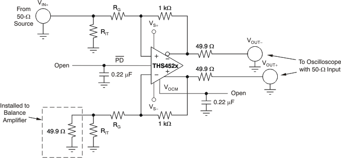 Figure 56. Slew Rate, Transient Response, Settling Time, Output Impedance, Overdrive Recovery, VOUT Swing, and Turn-On/Turn-Off Test Circuit
8.3.4 Common-Mode and Power-Supply Rejection
The circuit shown in Figure 57 is used to measure the CMRR. The signal from the network analyzer is applied common-mode to the input. Figure 58 is used to measure the PSRR of VS+ and VS–. The power supply under test is applied to the network analyzer dc offset input. For both CMRR and PSRR, the output is probed using a Tektronix high-impedance differential probe across the 953-Ω resistor and referred to the amplifier output by adding back the 0.42-dB as a result of the voltage divider on the output. For these tests, the resistors are matched for best results.
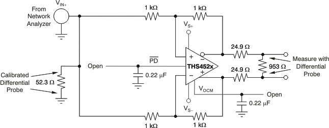 Figure 57. CMRR Test Circuit
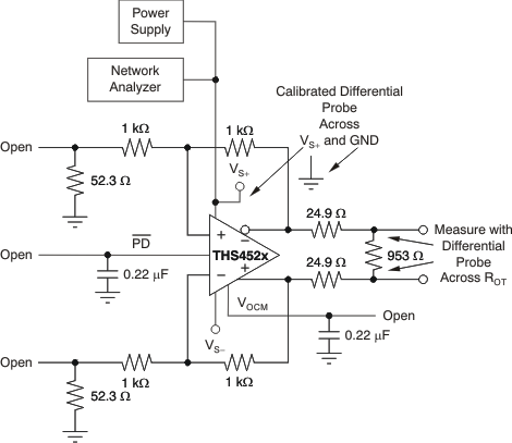 Figure 58. PSRR Test Circuit
8.3.5 VOCM Input
The circuit illustrated in Figure 59 is used to measure the frequency response and skew rate of the VOCM input. Frequency response is measured using a Tektronix high-impedance differential probe, with
RCM = 0 Ω at the common point of VOUT+ and VOUT–, formed at the summing junction of the two matched 499-Ω resistors, with respect to ground. The input impedance is measured using a Tektronix high-impedance differential probe at the VOCM input with RCM = 10 kΩ and the drop across the 10-kΩ resistor is used to calculate the impedance seen looking into the amplifier VOCM input.
The circuit shown in Figure 60 measures the transient response and slew rate of the VOCM input. A 1-V step input is applied to the VOCM input and the output is measured using a 50-Ω oscilloscope input referenced back to the amplifier output.
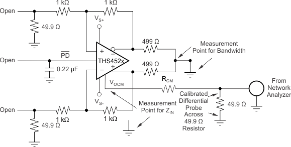 Figure 59. VOCM Input Test Circuit
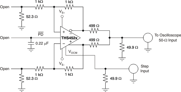 Figure 60. VOCM Transient Response and Slew Rate Test Circuit
8.3.6 Typical Performance Variation With Supply Voltage
The THS4521, THS4522, and THS4524 family of devices provide excellent performance across the specified power-supply range of 2.5 V to 5.5 V with only minor variations. The input and output voltage compliance ranges track with the power supply in nearly a 1:1 correlation. Other changes can be observed in slew rate, output current drive, open-loop gain, bandwidth, and distortion. Table 6 shows the typical variation to be expected in these key performance parameters.
8.3.7 Single-Supply Operation
To facilitate testing with common lab equipment, the THS4521EVM allows for split-supply operation; most of the characterization data presented in this data sheet is measured using split-supply power inputs. The device can easily be used with a single-supply power input without degrading performance.
Figure 61 shows a dc-coupled single-supply circuit with single-ended inputs. This circuit can also be applied to differential input sources.
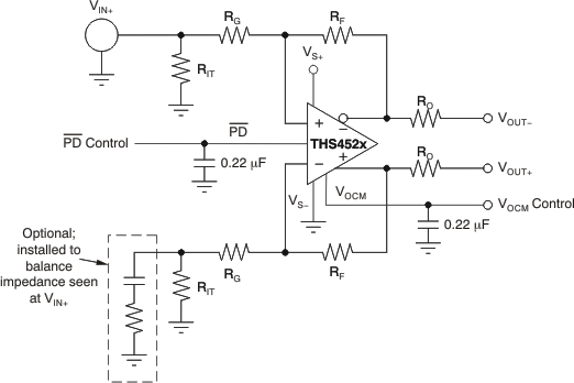 Figure 61. THS4521 DC-Coupled Single-Supply With Single-Ended Inputs
The input common-mode voltage range of the THS4521, THS4522, and THS4524 family is designed to include the negative supply voltage. in the circuit shown in Figure 61, the signal source is referenced to ground. VOCM is set by an external control source or, if left unconnected, the internal circuit defaults to midsupply. Together with the input impedance of the amplifier circuit, RIT provides input termination, which is also referenced to ground.
Note that RIT and optional matching components are added to the alternate input to balance the impedance at signal input.
Table 6. Typical Performance Variation Versus Power-Supply Voltage
| PARAMETER | VS = 5 V | VS = 3.3 V | VS = 2.5 V | |
|---|---|---|---|---|
| –3-dB Small-signal bandwidth | 145 MHz | 135 MHz | 125 MHz | |
| Slew rate (2-V step) | 490 V/μs | 420 V/μs | 210 V/μs | |
| Harmonic distortion at 1 MHz, 2 VPP, RL = 1 kΩ | Second harmonic | –85 dBc | –85 dBc | –84 dBc |
| Third harmonic | –91 dBc | –90 dBc | –88 dBc | |
| Open-loop gain (dc) | 119 dB | 116 dB | 115 dB | |
| Linear output current drive | 55 mA | 35 mA | 24 mA | |
8.3.8 Low-Power Applications and the Effects of Resistor Values on Bandwidth
For low-power operation, it may be necessary to increase the gain setting resistors values to limit current consumption and not load the source. Using larger value resistors lowers the bandwidth of the THS4521, THS4522, and THS4524 family as a result of the interactions between the resistors, the device parasitic capacitance, and printed circuit board (PCB) parasitic capacitance. Figure 62 shows the small-signal frequency response with 1-kΩ and 10-kΩ resistors for RF, RG, and RL (impedance is assumed to typically increase for all three resistors in low-power applications).
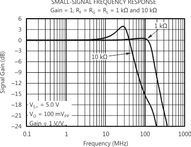 Figure 62. THS4521 Frequency Response With Various Gain Setting and Load Resistor Values
8.3.9 Frequency Response Variation due to Package Options
Users can see variations in the small-signal (VOUT = 100 mVPP) frequency response between the available package options for the THS4521, THS4522, and THS4524 family as a result of parasitic elements associated with each package and board layout changes. Figure 63 shows the variance measured in the lab; this variance is to be expected even when using a good layout.
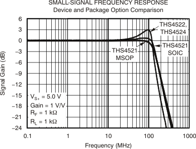 Figure 63. Small-Signal Frequency Response: Package Variations
8.3.10 Driving Capacitive Loads
The THS4521, THS4522, and THS4524 family is designed for a nominal capacitive load of 1 pF on each output to ground. When driving capacitive loads greater than 1 pF, it is recommended to use small resistors (RO) in series with the output, placed as close to the device as possible. Without RO, capacitance on the output interacts with the output impedance of the amplifier and causes phase shift in the loop gain of the amplifier that reduces the phase margin. This reduction in phase margin results in frequency response peaking; overshoot, undershoot, and/or ringing when a step or square-wave signal is applied; and may lead to instability or oscillation. Inserting RO isolates the phase shift from the loop gain path and restores the phase margin, but it also limits bandwidth. Figure 64 shows the recommended values of RO versus capacitive loads (CL), and Figure 65 shows an illustration of the frequency response with various values.
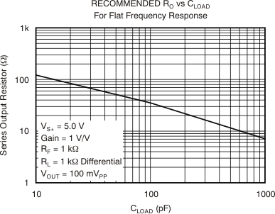 Figure 64. Recommended Series Output Resistor Versus Capacitive Load for Flat Frequency Response, With RLOAD = 1 kΩ
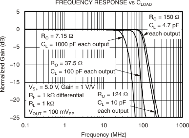 Figure 65. Frequency Response for Various RO and CL Values, With RLOAD = 1 kΩ
8.3.11 Audio Performance
The THS4521, THS4522, and THS4524 family provide excellent audio performance with very low quiescent power. To show performance in the audio band, the device was tested with a SYS-2722 audio analyzer from Audio Precision. THD+N and FFT tests were performed at 1-VRMS output voltage. Performance is the same on both 3.3-V and 5-V supplies. Figure 66 shows the test circuit used; see Figure 67 and Figure 68 for the performance of the analyzer using internal loopback mode (generator) together with the THS4521.
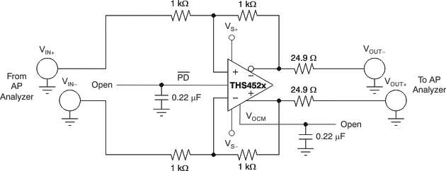 Figure 66. THS4521 AP Analyzer Test Circuit
Note that the harmonic distortion performance is very close to the same with and without the device meaning the THS4521 performance is actually much better than can be directly measured by this method. The actual device performance can be estimated by placing the device in a large noise gain and using the reduction in loop gain correction. The THS4521 is placed in a noise gain of 101 by adding a 10-Ω resistor directly across the input terminals of the circuit shown in Figure 66. This test was performed using the AP instrument as both the signal source and the analyzer. The second-order harmonic distortion at 1 kHz is estimated to be –122 dBc with VO = 1VRMS; third-order harmonic distortion is estimated to be –141 dBc. The third-order harmonic distortion result matches exactly with design simulations, but the second-order harmonic distortion is about 10 dB worse. This result is not unexpected because second-order harmonic distortion performance with a differential signal depends heavily on cancellation as a result of the differential nature of the signal, which depends on board layout, bypass capacitors, external cabling, and so forth. Note that the circuit of Figure 66 is also used to measure crosstalk between channels.
The THS4521 shows even better THD+N performance when driving higher amplitude output, such as 5 VPP that is more typical when driving an ADC. To show performance with an extended frequency range, higher gain, and higher amplitude, the device was tested with 5 VPP up to 80 kHz with the AP. Figure 69 shows the resulting THD+N graph with no weighting.
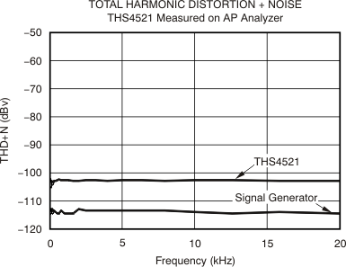 Figure 67. THS4521 1-VRMS 20-Hz to 20-kHz Thd+N
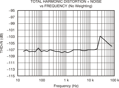 Figure 69. Thd+N (No Weighting) on Ap, 80-kHz Bandwidth at G = 1 With 5-VPP Output
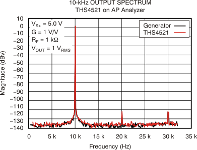 Figure 68. THS4521 1-VRMS 10-kHz FFT Plot
8.3.12 Audio On/Off Pop Performance
The THS4521 was tested to show on and off pop performance by connecting a speaker between the differential outputs and switching the power supply on and off, and also by using the PD function of the THS4521. Testing was done with and without tones. During these tests, no audible pop could be heard.
With no tone input, Figure 70 shows the pop performance when switching power on to the THS4521 and Figure 71 shows the device performance when turning the power off. The transients during power on and off illustrate that no audible pop should be heard
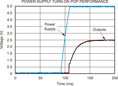 Figure 70. THS4521 Power-Supply Turn-On Pop Performance
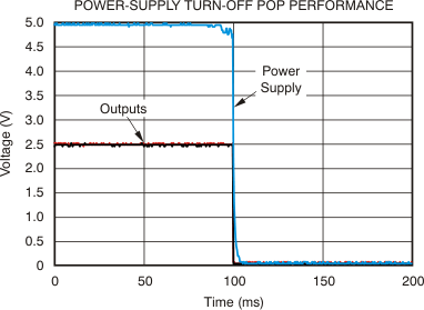 Figure 71. THS4521 Power-Supply Turn-Off Pop Performance
With no tone input, Figure 72 shows the pop performance using the PD pin to enable the THS4521, and Figure 73 shows performance using the PD pin to disable the device. Again, the transients during power on and off show that no audible pop should be heard. It should also be noted that the turn on/off times are faster using the PD pin technique.
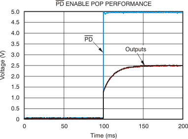 Figure 72. THS4521 PD Pin Enable Pop Performance
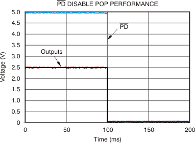 Figure 73. THS4521 PD Pin Disable Pop Performance
The power on/off pop performance of the THS4521, whether by switching the power supply or when using the power-down function built into the chip, shows that no special design should be required to prevent an audible pop.
8.4 Device Functional Modes
This wideband FDA requires external resistors for correct signal-path operation. When configured for the desired input impedance and gain setting with these external resistors, the amplifier can be either on with the PD pin asserted to a voltage greater than VS– + 1.7 V, or turned off by asserting PD low. Disabling the amplifier shuts off the quiescent current and stops correct amplifier operation. The signal path is still present for the source signal through the external resistors.
The VOCM control pin sets the output average voltage. Left open, VOCM defaults to an internal midsupply value. Driving this high-impedance input with a voltage reference within its valid range sets a target for the internal VCM error amplifier.
8.4.1 Operation from Single-Ended Sources to Differential Outputs
One of the most useful features supported by the FDA device is an easy conversion from a single-ended input to a differential output centered on a user-controlled, common-mode level. While the output side is relatively straightforward, the device input pins move in a common-mode sense with the input signal. This common-mode voltage at the input pins moving with the input signal acts to increase the apparent input impedance to be greater than the RG value. This input-active-impedance issue applies to both ac- and dc-coupled designs, and requires somewhat more complex solutions for the resistors to account for this active impedance, as shown in the following subsections.
8.4.1.1 AC-Coupled Signal Path Considerations for Single-Ended Input to Differential Output Conversion
When the signal path can be ac-coupled, the dc biasing for the THS452x family becomes a relatively simple task. In all designs, start by defining the output common-mode voltage. The ac-coupling issue can be separated for the input and output sides of an FDA design. The input can be ac-coupled and the output dc-coupled, or the output can be ac-coupled and the input dc-coupled, or they can both be ac-coupled.
One situation where the output might be dc-coupled (for an ac-coupled input), is when driving directly into an ADC where the VOCM control voltage uses the ADC common-mode reference to directly bias the FDA output common-mode to the required ADC input common-mode. In any case, the design starts by setting the desired VOCM.
When an ac-coupled path follows the output pins, the best linearity is achieved by operating VOCM at midsupply. The VOCM voltage must be within the linear range for the common-mode loop, as specified in the headroom specifications (approximately 0.91 V greater than the negative supply and 1.1 V less than the positive supply). If the output path is also ac-coupled, simply letting the VOCM control pin float is usually preferred in order to get a midsupply default VOCM bias with minimal elements. To limit noise, place a 0.1-µF decoupling capacitor on the VOCM pin to ground.
After VOCM is defined, check the target output voltage swing to ensure that the VOCM plus the positive or negative output swing on each side do not clip into the supplies. If the desired output differential swing is defined as VOPP, divide by 4 to obtain the ±VP swing around VOCM at each of the two output pins (each pin operates 180° out of phase with the other). Check that VOCM ±VP does not exceed the absolute supply rails for this rail-to-rail output (RRO) device.
Going to the device input pins side, because both the source and balancing resistor on the non-signal input side are dc-blocked (see Figure 74), no common-mode current flows from the output common-mode voltage, thus setting the input common-mode equal to the output common-mode voltage.
This input headroom also sets a limit for higher VOCM voltages. Because the input VICM is the output VOCM for ac-coupled sources, the 1.2-V minimum headroom for the input pins to the positive supply overrides the 1.1-V headroom limit for the output VOCM. Also, the input signal moves this input VICM around the dc bias point, as described in the section Resistor Design Equations for the Single-Ended to Differential Configuration of the FDA.
 Figure 74. AC-coupled, Single-ended Source to a Differential Gain of 2 V/V Test Circuit
8.4.1.2 DC-Coupled Input Signal Path Considerations for Single-Ended to Differential Conversion
The output considerations remain the same as for the ac-coupled design. Again, the input can be dc-coupled while the output is ac-coupled. A dc-coupled input with an ac-coupled output might have some advantages to move the input VICM down if the source is ground referenced. When the source is dc-coupled into the THS452x family (see Figure 75 ), both sides of the input circuit must be dc-coupled to retain differential balance. Normally, the non-signal input side has an RG element biased to whatever the source midrange is expected to be. Providing this midscale reference gives a balanced differential swing around VOCM at the outputs.
Often, RG2 is simply grounded for dc-coupled, bipolar-input applications. This configuration gives a balanced differential output if the source is swinging around ground. If the source swings from ground to some positive voltage, grounding RG2 gives a unipolar output differential swing from both outputs at VOCM (when the input is at ground) to one polarity of swing. Biasing RG2 to an expected midpoint for the input signal creates a differential output swing around VOCM.
One significant consideration for a dc-coupled input is that VOCM sets up a common-mode bias current from the output back through RF and RG to the source on both sides of the feedback. Without input balancing networks, the source must sink or source this dc current. After the input signal range and biasing on the other RG element is set, check that the voltage divider from VOCM to VIN through RF and RG (and possibly RS) establishes an input VICM at the device input pins that is in range.
If the average source is at ground, the negative rail input stage for the THS452x family is in range for applications using a single positive supply and a positive output VOCM setting because this dc current lifts the average FDA input summing junctions up off of ground to a positive voltage (the average of the V+ and V– input pin voltages on the FDA).
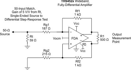 Figure 75. DC-Coupled, Single-Ended-to-Differential, Set for a Gain of 5 V/V
8.4.1.3 Resistor Design Equations for the Single-Ended to Differential Configuration of the FDA
The design equations for setting the resistors around an FDA to convert from a single-ended input signal to differential output can be approached from several directions. Here, several critical assumptions are made to simplify the results:
- The feedback resistors are selected first and set equal on the two sides.
- The dc and ac impedances from the summing junctions back to the signal source and ground (or a bias voltage on the non-signal input side) are set equal to retain feedback divider balance on each side of the FDA.
Both of these assumptions are typical for delivering the best dynamic range through the FDA signal path.
After the feedback resistor values are chosen, the aim is to solve for the RT (a termination resistor to ground on the signal input side), RG1 (the input gain resistor for the signal path), and RG2 (the matching gain resistor on the nonsignal input side); see Figure 74 and Figure 75. The same resistor solutions can be applied to either ac- or dc-coupled paths. Adding blocking capacitors in the input-signal chain is a simple option. Adding these blocking capacitors after the RT element (as shown in Figure 74) has the advantage of removing any dc currents in the feedback path from the output VOCM to ground.
Earlier approaches to the solutions for RT and RG1 (when the input must be matched to a source impedance, RS) follow an iterative approach. This complexity arises from the active input impedance at the RG1 input. When the FDA is used to convert a single-ended signal to differential, the common-mode input voltage at the FDA inputs must move with the input signal to generate the inverted output signal as a current in the RG2 element. A more recent solution is shown as Equation 1, where a quadratic in RT can be solved for an exact value. This quadratic emerges from the simultaneous solution for a matched input impedance and target gain. The only inputs required are:
- The selected RF value.
- The target voltage gain (Av) from the input of RT to the differential output voltage.
- The desired input impedance at the junction of RT and RG1 to match RS.
Solving this quadratic for RT starts the solution sequence, as shown in Equation 1:

Being a quadratic, there are limits to the range of solutions. Specifically, after RF and RS are chosen, there is physically a maximum gain beyond which Equation 1 starts to solve for negative RT values (if input matching is a requirement). With RF selected, use Equation 2 to verify that the maximum gain is greater than the desired gain.
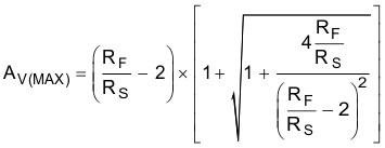
If the achievable AV(MAX) is less than desired, increase the RF value. After RT is derived from Equation 1, the RG1 element is given by Equation 3:
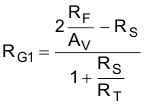
Then, the simplest approach is to use a single RG2 = RT || RS + RG1 on the non-signal input side. Often, this approach is shown as the separate RG1 and RS elements. Using these separate elements provides a better divider match on the two feedback paths, but a single RG2 is often acceptable. A direct solution for RG2 is given as Equation 4:
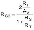
This design proceeds from a target input impedance matched to RS, signal gain Av from the matched input to the differential output voltage, and a selected RF value. The nominal RF value chosen for the THS452x family characterization is 402 Ω. As discussed previously, going lower improves noise and phase margin, but reduces the total output load impedance possibly degrading harmonic distortion. Going higher increases the output noise, and might reduce the loop-phase margin because of the feedback pole to the input capacitance, but reduces the total loading on the outputs.
Using Equation 2 to Equation 4 to sweep the target gain from 1 to AV(MAX) < 14.3 V/V gives Table 7, which shows exact values for RT, RG1, and RG2, where a 50-Ω source must be matched while setting the two feedback resistors to 402 Ω. One possible solution for 1% standard values is shown, and the resulting actual input impedance and gain with % errors to the targets are also shown in Table 7.
Table 7. Rf = 1 kΩ, Matched Input to 50 Ω, Gain from 1 V to 10 V/V Single to Differential(1)
| Av | Rt, EXACT (Ω) | Rt 1% | Rg1, EXACT (Ω) | Rg1 1% | Rg2, EXACT (Ω) | Rg2 1% | ACTUAL ZIN | %ERR TO Rs | ACTUAL GAIN | %ERR TO Av |
|---|---|---|---|---|---|---|---|---|---|---|
| 1 | 51.95 | 52.3 | 996.92 | 1000 | 1022.48 | 1020 | 50.32 | 0.64% | 0.997 | –0.30% |
| 2 | 53.59 | 53.6 | 491.51 | 487 | 517.37 | 523 | 49.95 | –0.10% | 2.018 | 0.88% |
| 3 | 55.21 | 54.9 | 322.74 | 324 | 348.90 | 348 | 49.70 | –0.60% | 2.989 | –0.36% |
| 4 | 56.88 | 56.2 | 238.14 | 237 | 264.60 | 267 | 49.37 | –1.25% | 4.017 | 0.43% |
| 5 | 58.63 | 59 | 189.45 | 191 | 216.51 | 215 | 50.23 | 0.47% | 4.964 | –0.71% |
| 6 | 60.47 | 60.4 | 155.01 | 154 | 182.37 | 182 | 49.82 | –0.37% | 6.033 | 0.56% |
| 7 | 62.42 | 61.9 | 130.39 | 130 | 158.05 | 158 | 49.51 | –0.98% | 7.017 | 0.25% |
| 8 | 64.49 | 64.9 | 112.97 | 113 | 141.21 | 140 | 50.12 | 0.23% | 7.998 | –0.02% |
| 9 | 66.70 | 66.5 | 98.31 | 97.6 | 126.85 | 127 | 49.69 | –0.62% | 9.050 | 0.56% |
| 10 | 69.06 | 69.8 | 87.40 | 86.6 | 116.53 | 118 | 50.29 | 0.57% | 10.069 | 0.69% |
These equations and design flow apply to any FDA. Using the feedback resistor value as a starting point is particularly useful for current-feedback-based FDAs such as the LMH6554, where the value of these feedback resistors determines the frequency response flatness. Similar tables can be built using the equations provided here for other source impedances, RF values, and gain ranges.
The TINA model correctly shows this actively-set input impedance in the single-ended to differential configuration, and is a good tool to validate the gains, input impedances, response shapes, and noise issues.
8.4.1.4 Input Impedance for the Single-Ended to Differential FDA Configuration
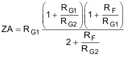
The designs so far have included a source impedance, RS, that must be matched by RT and RG1. The total impedance at the junction of RT and RG1 for the circuit of Figure 75 is the parallel combination of RT to ground, and the ZA (active impedance) presented by RG1. The expression for ZA, assuming RG2 is set to obtain the differential divider balance, is given by Equation 5:
For designs that do not need impedance matching, for instance where the input is driven from the low-impedance output of another amplifier, RG1 = RG2 is the single-to-differential design used without an RT to ground. Setting RG1 = RG2 = RG in Equation 5 produces Equation 6, which is the input impedance of a simple-input FDA driven from a low-impedance, single-ended source.
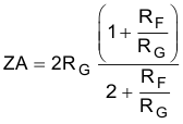
In this case, setting a target gain as RF / RG ≡ α, and then setting the desired input impedance allows the RG element to be resolved first. Then the RF is set to get the target gain. For example, targeting an input impedance of 200 Ω with a gain of 4 V/V, Equation 7 calculates the RG value. Multiplying this required RG value by a gain
of 4 gives the RF value and the design of Figure 76.

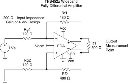 Figure 76. 200-Ω Input Impedance, Single-Ended to Differential DC-Coupled Design With Gain of 4 V/V
After being designed, this circuit can also be ac-coupled by adding blocking caps in series with the two 120-Ω RG resistors. This active input impedance has the advantage of increasing the apparent load to the prior stage using lower resistors values, leading to lower output noise for a given gain target.
8.4.2 Differential-Input to Differential-Output Operation
In many ways, this method is a much simpler way to operate the FDA from a design-equations perspective. Again, assuming the two sides of the circuit are balanced with equal RF and RG elements, the differential input impedance is now just the sum of the two RG elements to a differential inverting summing junction. In these designs, the input common-mode voltage at the summing junctions does not move with the signal, but must be dc biased in the allowable range for the input pins with consideration given to the voltage headroom required from each supply. Slightly different considerations apply to ac- or dc-coupled, differential-in to differential-out designs, as described in the following sections.
8.4.2.1 AC-Coupled, Differential-Input to Differential-Output Design Issues
There are two typical ways to use the THS452x family with an ac-coupled differential source. In the first method, the source is differential and can be coupled in through two blocking capacitors. The second method uses either a single-ended or a differential source and couples in through a transformer (or balun). Figure 77 shows a typical blocking capacitor approach to a differential input. An optional differential-input termination resistor (RM) is included in this design. This RM element allows the input RG resistors to be scaled up while still delivering lower differential input impedance to the source. In this example, the RG elements sum to show a 500-Ω differential impedance, while the RM element combines in parallel to give a net 100-Ω, ac-coupled, differential impedance to the source. Again, the design proceeds ideally by selecting the RF element values, then the RG to set the differential gain, then an RM element (if needed) to achieve the target input impedance. Alternatively, the RM element can be eliminated, the RG elements set to the desired input impedance, and RF set to the get the differential gain (RF / RG).
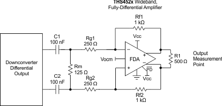 Figure 77. Example Down-Converting Mixer Delivering an AC-Coupled Differential Signal to the THS452x
The dc biasing here is very simple. The output VOCM is set by the input control voltage; and because there is no dc-current path for the output common-mode voltage, that dc bias also sets the input pins common-mode operating points.
8.5 Programming
8.5.1 Input Common-Mode Voltage Range
The input common-mode voltage of a fully-differential amplifier is the voltage at the + and – input pins of the device.
It is important to not violate the input common-mode voltage range (VICR) of the amplifier. Assuming the amplifier is in linear operation, the voltage across the input pins is only a few millivolts at most. Therefore, finding the voltage at one input pin determines the input common-mode voltage of the amplifier.
Treating the negative input as a summing node, the voltage is given by Equation 8:

To determine the VICR of the amplifier, the voltage at the negative input is evaluated at the extremes of VOUT+. As the gain of the amplifier increases, the input common-mode voltage becomes closer and closer to the input common-mode voltage of the source.
8.5.1.1 Setting the Output Common-Mode Voltage
The output common-model voltage is set by the voltage at the VOCM pin. The internal common-mode control circuit maintains the output common-mode voltage within 5-mV offset (typ) from the set voltage. If left unconnected, the common-mode set point is set to midsupply by internal circuitry, which may be overdriven from an external source.
Figure 78 represents the VOCM input. The internal VOCM circuit has typically 23 MHz of –3 dB bandwidth, which is required for best performance, but it is intended to be a dc bias input pin. A 0.22-μF bypass capacitor is recommended on this pin to reduce noise. The external current required to overdrive the internal resistor divider is given approximately by the formula in Equation 9:

where
- VOCM is the voltage applied to the VOCM pin
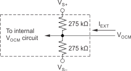 Figure 78. VOCM Input Circuit