SLOS358C September 2011 – April 2020 THS4531
PRODUCTION DATA.
- 1 Features
- 2 Applications
- 3 Description
- 4 Revision History
- 5 Packaging and Ordering Information
- 6 Electrical Specifications
- 7 Device Information
- 8 Table of Graphs
- 9 Typical Characteristics: VS = 2.7 V
- 10Typical Characteristics: VS = 5 V
-
11Application Information
- 11.1 Typical Characteristics Test Circuits
- 11.2
Application Circuits
- 11.2.1 Differential Input to Differential Output Amplifier
- 11.2.2 Single-Ended Input to Differential Output Amplifier
- 11.2.3 Differential Input to Single-Ended Output Amplifier
- 11.2.4 Input Common-Mode Voltage Range
- 11.2.5 Setting the Output Common-Mode Voltage
- 11.2.6 Single-Supply Operation
- 11.2.7 Low Power Applications and the Effects of Resistor Values on Bandwidth
- 11.2.8 Driving Capacitive Loads
- 11.2.9 Audio Performance
- 11.2.10 Audio On and Off Pop Performance
- 11.3 Audio ADC Driver Performance: THS4531 AND PCM4204 Combined Performance
- 11.4 SAR ADC Performance
- 11.5 EVM and Layout Recommendations
- 12Device and Documentation Support
- 13Mechanical, Packaging, and Orderable Information
パッケージ・オプション
メカニカル・データ(パッケージ|ピン)
サーマルパッド・メカニカル・データ
- RUN|10
発注情報
11.1.4 Common-Mode and Power Supply Rejection
The circuit shown in Figure 69 is used to measure the CMRR. The signal from the network analyzer is applied common-mode to the input.
 Figure 69. CMRR Test Circuit
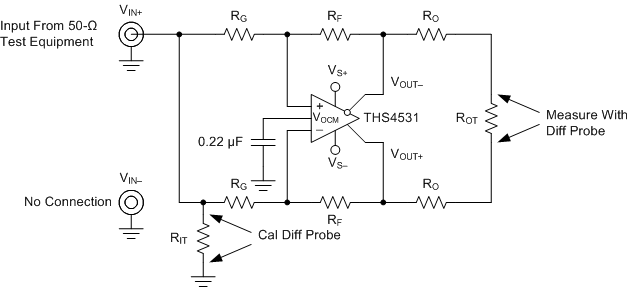
 Figure 70 is used to measure the PSRR of VS+ and VS-. The power supply is applied to the network analyzer’s DC offset input. For both CMRR and PSRR, the output is probed using a high impedance differential probe across ROT.
 Figure 70. PSRR Test Circuit