SLOS358C September 2011 – April 2020 THS4531
PRODUCTION DATA.
- 1 Features
- 2 Applications
- 3 Description
- 4 Revision History
- 5 Packaging and Ordering Information
- 6 Electrical Specifications
- 7 Device Information
- 8 Table of Graphs
- 9 Typical Characteristics: VS = 2.7 V
- 10Typical Characteristics: VS = 5 V
-
11Application Information
- 11.1 Typical Characteristics Test Circuits
- 11.2
Application Circuits
- 11.2.1 Differential Input to Differential Output Amplifier
- 11.2.2 Single-Ended Input to Differential Output Amplifier
- 11.2.3 Differential Input to Single-Ended Output Amplifier
- 11.2.4 Input Common-Mode Voltage Range
- 11.2.5 Setting the Output Common-Mode Voltage
- 11.2.6 Single-Supply Operation
- 11.2.7 Low Power Applications and the Effects of Resistor Values on Bandwidth
- 11.2.8 Driving Capacitive Loads
- 11.2.9 Audio Performance
- 11.2.10 Audio On and Off Pop Performance
- 11.3 Audio ADC Driver Performance: THS4531 AND PCM4204 Combined Performance
- 11.4 SAR ADC Performance
- 11.5 EVM and Layout Recommendations
- 12Device and Documentation Support
- 13Mechanical, Packaging, and Orderable Information
パッケージ・オプション
メカニカル・データ(パッケージ|ピン)
サーマルパッド・メカニカル・データ
- RUN|10
発注情報
11.2.8 Driving Capacitive Loads
The THS4531 is designed for a nominal capacitive load of 2 pF (differentially). When driving capacitive loads greater than this, it is recommended to use small resisters (RO) in series with the output as close to the device as possible. Without RO, capacitance on the output will interact with the output impedance of the amplifier causing phase shift in the loop gain of the amplifier that will reduce the phase margin resulting in:
1. Peaking in the frequency response.
2. Overshoot, undershoot, and ringing in the time domain response with a pulse or square-wave signal.
3. May lead to instability or oscillation.
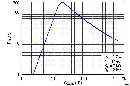
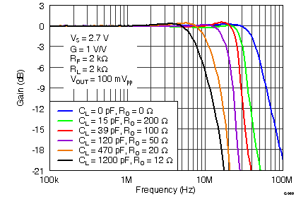
Inserting RO will compensate the phase shift and restore the phase margin, but it will also limit bandwidth. The circuit shown in Figure 68 is used to test for best RO versus capacitive loads, CL, with a capacitance placed differential across the VOUT+ and VOUT- along with 2 kΩ load resistor, and the output is measure with a differential probe. Figure 77 shows the optimum values of RO versus capacitive loads, CL, and Figure 78 shows the frequency response with various values. Performance is the same on both 2.7 V and 5 V supply.
 Figure 77. Recommended Series Output Resistor vs Capacitive Load for Flat Frequency Response
  Figure 78. Frequency Response for Various RO and CL Values