JAJSL64D April 2016 – June 2021 THS4551
PRODUCTION DATA
- 1 特長
- 2 アプリケーション
- 3 概要
- 4 Revision History
- 5 Companion Devices
- 6 Pin Configuration and Functions
-
7 Specifications
- 7.1 Absolute Maximum Ratings
- 7.2 ESD Ratings
- 7.3 Recommended Operating Conditions
- 7.4 Thermal Information
- 7.5 Electrical Characteristics: (VS+) – (VS–) = 5 V
- 7.6 Electrical Characteristics: (VS+) – (VS–) = 3 V
- 7.7 Typical Characteristics: (VS+) – (VS–) = 5 V
- 7.8 Typical Characteristics: (VS+) – (VS–) = 3 V
- 7.9 Typical Characteristics: 3-V to 5-V Supply Range
-
8 Parameter Measurement Information
- 8.1 Example Characterization Circuits
- 8.2 Output Interface Circuit for DC-Coupled Differential Testing
- 8.3 Output Common-Mode Measurements
- 8.4 Differential Amplifier Noise Measurements
- 8.5 Balanced Split-Supply Versus Single-Supply Characterization
- 8.6 Simulated Characterization Curves
- 8.7 Terminology and Application Assumptions
- 9 Detailed Description
- 10Application and Implementation
- 11Power Supply Recommendations
- 12Layout
- 13Device and Documentation Support
- 14Mechanical, Packaging, and Orderable Information
パッケージ・オプション
メカニカル・データ(パッケージ|ピン)
サーマルパッド・メカニカル・データ
発注情報
10.2.2 Differential Transimpedance Output to a High-Grade Audio PCM DAC Application
The highest-grade audio digital-to-analog converters (DACs) are a differential current-mode output. These devices normally suggest a two-amplifier transimpedance stage to hold the DAC output voltages fixed when the amplifiers produce a differential voltage swing at the outputs. Often, the differential voltage swing is then converted to single-ended in a differencing amplifier stage to drive headphone loads (see Figure 35 in the OPA1611). The emerging high-power class D audio amplifiers often require differential inputs. Applying the THS4551 as a differential transimpedance stage offers a simple solution for very low-distortion, differential-output audio channels.
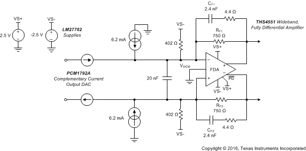
Starting with the output specifications for a very high-performance PCM1792A audio DAC, the requirements for the THS4551 interface can be extracted. The DAC is a current-sourcing device that requires its outputs to be held at ground when using a transimpedance amplifier. Using the DAC 3.3-V supply and the LM27762 low-noise, low-dropout (LDO) regulator and inverter provides a ±2.5-V supply to the THS4551. Operating the THS4551 on ±2.5-V supplies places all nodes in range for an input VCM equal to GND (and the DAC output voltages as well) and an FDA output VOCM also equal to GND.
The center current in Table 10-2 is a fixed 6.2-mA dc current coming out of the DAC outputs regardless of the DAC code. This dc common-mode current can be absorbed by the –2.5-V supply at the input pins to hold the DAC compliance voltage and FDA input pins at ground. The FDA controls the output common-mode voltage, set to ground in this case, whereas the input pin voltage (which does not move with the DAC output differential current) is controlled with a resistor to the negative supply.
| ANALOG OUTPUT | TEST CONDITION | MIN | TYP | MAX | UNIT |
|---|---|---|---|---|---|
| Gain error | –6 | ±2 | 6 | % of FSR | |
| Gain mismatch, channel-to-channel | –3 | ±0.5 | 3 | % of FSR | |
| Bipolar zero (BPZ) error | At BPZ | –2 | ±0.5 | 2 | % of FSR |
| Output current | Full-scale (0 dB) | 7.8 | mAPP | ||
| Center current | At BPZ | –6.2 | mA |
This bias is provided by the 402-Ω resistors to –2.5 V, as illustrated in Figure 10-14. This design takes the differential 7.8 mAPP from the DAC and produces a ±1.46-V swing on each output of the THS4551. This configuration gives a full-scale differential 5.85 VPP available on the ±2.5-V supply design centered at ground at both the inputs and outputs. Although the LM27762 provides a very-low noise, –2.5-V supply, using 0.1% resistors in the current sink path to the –2.5-V supply as well as the feedback resistors limits any common-mode noise on the –2.5-V supply to differential mode conversion at the FDA outputs.
 Figure 10-14 PCM1792A DAC Output
Driver