SBOS431A May 2009 – March 2017 THS6214
PRODUCTION DATA.
- 1 Features
- 2 Applications
- 3 Description
- 4 Revision History
- 5 Pin Configuration and Functions
-
6 Specifications
- 6.1 Absolute Maximum Ratings
- 6.2 ESD Ratings
- 6.3 Recommended Operating Conditions
- 6.4 Thermal Information
- 6.5 Electrical Characteristics: VS = ±12 V
- 6.6 Electrical Characteristics: VS = ±6 V
- 6.7 Timing Requirements
- 6.8 Typical Characteristics: VS = ±12 V, Full Bias
- 6.9 Typical Characteristics: VS = ±12 V, Mid Bias
- 6.10 Typical Characteristics: VS = ±12 V, Low Bias
- 6.11 Typical Characteristics: VS = ±6 V, Full Bias
- 6.12 Typical Characteristics: VS = ±6 V, Mid Bias
- 6.13 Typical Characteristics: VS = ±6 V, Low Bias
- 7 Detailed Description
- 8 Application and Implementation
- 9 Power Supply Recommendations
- 10Layout
- 11Device and Documentation Support
- 12Mechanical, Packaging, and Orderable Information
パッケージ・オプション
メカニカル・データ(パッケージ|ピン)
サーマルパッド・メカニカル・データ
- PWP|24
発注情報
7 Detailed Description
7.1 Overview
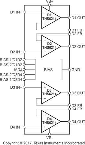
The THS6214 is a differential line-driver amplifier with a current-feedback architecture. The device is targeted for use in line-driver applications (such as xDSL and wide-band, power-line communications) and is fast enough to support transmissions of 14.5-dBm line power up to 30 MHz. The architecture of the THS6214 is designed to provide maximum flexibility with multiple bias settings that are selectable based on application performance requirements, and also provides an external current pin (IADJ) to further adjust the bias current to the device. The wide output swing (43.2 VPP) and high current drive (416 mA) of the THS6214 make the device ideally suited for high-power, line-driving applications.
7.2 Functional Block Diagram

7.3 Feature Description
7.3.1 Output Current and Voltage
The THS6214 provides output voltage and current capabilities that are unsurpassed in a low-cost, dual monolithic op amp. Under no-load conditions at 25°C, the output voltage typically swings closer than 1.1 V to either supply rail; tested at 25°C, the swing limit is within 1.4 V of either rail into a 100-Ω differential load. Into a 25-Ω load (the minimum tested load), the amplifier delivers more than ±408-mA continuous and greater than ±1-A peak output current.
The specifications described in the previous paragraph, though familiar in the industry, consider voltage and current limits separately. In many applications, the voltage times current (or V-I product) is more relevant to circuit operation. See the Output Voltage and Current Limitations plot (Figure 13) in the Typical Characteristics section. The X- and Y-axes of this graph show the zero-voltage output current limit and the zero-current output voltage limit, respectively. The four quadrants give a more detailed view of the THS6214 output drive capabilities, noting that the graph is bounded by a safe operating area of 1-W maximum internal power dissipation (in this case, for one channel only). Superimposing resistor load lines onto the plot illustrates that the THS6214 can drive ±10.9 V into 100 Ω or ±10.5 V into 50 Ω without exceeding the output capabilities or the 1-W dissipation limit. A 100-Ω load line (the standard test circuit load) illustrates the full ±12-V output swing capability, as provided in the Electrical Characteristics tables. The minimum specified output voltage and current over temperature are set by worst-case simulations at the cold temperature extreme. Only at cold startup do the output current and voltage decrease to the numbers provided in the Electrical Characteristics tables. When the output transistors deliver power, the junction temperature increases, decreasing the VBEs (increasing the available output voltage swing), and increasing the current gains (increasing the available output current). In steady-state operation, the available output voltage and current are always greater than that shown in the overtemperature specifications, because the output stage junction temperatures are higher than the minimum specified operating ambient temperature. To maintain maximum output stage linearity, no output short-circuit protection is provided. This absence of short-circuit protection is normally not a problem because most applications include a series-matching resistor at the output that limits the internal power dissipation if the output side of this resistor is shorted to ground. However, shorting the output pin directly to the adjacent positive power-supply pin (24-pin package), in most cases destroys the amplifier. If additional short-circuit protection is required, a small series resistor can be included in the supply lines. Under heavy output loads, this additional resistor reduces the available output voltage swing. A 5-Ω series resistor in each power-supply lead limits the internal power dissipation to less than 1 W for an output short-circuit, and decreases the available output voltage swing only 0.5 V for up to 100-mA desired load currents. Always place the 0.1-µF power-supply decoupling capacitors after these supply current limiting resistors, directly on the supply pins.
7.3.2 Driving Capacitive Loads
One of the most demanding and yet very common load conditions for an op amp is capacitive loading. Often, the capacitive load is the input of an ADC—including additional external capacitance that may be recommended to improve the ADC linearity. A high-speed, high open-loop gain amplifier such as the THS6214 can be very susceptible to decreased stability and closed-loop response peaking when a capacitive load is placed directly on the output pin. When the amplifier open-loop output resistance is considered, this capacitive load introduces an additional pole in the signal path that can decrease the phase margin. Several external solutions to this problem have been suggested below.
When the primary considerations are frequency response flatness, pulse response fidelity, and distortion, the simplest and most effective solution is to isolate the capacitive load from the feedback loop by inserting a series isolation resistor between the amplifier output and the capacitive load. This series resistor does not eliminate the pole from the loop response, but shifts the pole and adds a zero at a higher frequency. The additional zero functions to cancel the phase lag from the capacitive load pole, thus increasing the phase margin and improving stability. The Typical Characteristics illustrate the recommended RS versus capacitive load (see Figure 5, Figure 23, Figure 35, Figure 47, Figure 60, and Figure 72) and the resulting frequency response at the load. Parasitic capacitive loads greater than 2 pF can begin to degrade device performance. Long printed-circuit board (PCB) traces, unmatched cables, and connections to multiple devices can easily cause this value to be exceeded. Always consider this effect carefully, and add the recommended series resistor as close as possible to the THS6214 output pin (see the Board Layout Guidelines section).
7.3.3 Distortion Performance
The THS6214 provides good distortion performance into a 100-Ω load on ±12-V supplies. Relative to alternative solutions, the amplifier provides exceptional performance into lighter loads and operation on a dual ±6-V supply. Generally, until the fundamental signal reaches very high frequency or power levels, the second harmonic dominates the distortion with a negligible third-harmonic component. Focusing then on the second harmonic, increasing the load impedance improves distortion directly. Remember that the total load includes the feedback network—in the noninverting configuration (see Figure 81), this value is the sum of RF + RG, whereas in the inverting configuration this value is just RF. Also, providing an additional supply decoupling capacitor (0.01 µF) between the supply pins (for bipolar operation) improves the second-order distortion slightly (from 3 dB to 6 dB).
In most op amps, increasing the output voltage swing directly increases harmonic distortion. The Typical Characteristics illustrate the second harmonic increasing at a little less than the expected 2x rate, whereas the third harmonic increases at a little less than the expected 3x rate. Where the test power doubles, the second harmonic decreases less than the expected 6 dB, and the third harmonic decreases by less than the expected 12 dB. This difference also appears in the two-tone, third-order intermodulation spurious (IM3) response curves. The third-order spurious levels are extremely low at low-output power levels, and the output stage continues to hold them low even when the fundamental power reaches very high levels.
7.3.4 Differential Noise Performance
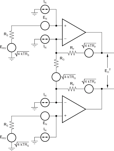
The THS6214 is designed to be used as a differential driver in xDSL applications. Therefore, analyzing the noise in such a configuration is important. Figure 80 shows the op amp noise model for the differential configuration.
 Figure 80. Differential Op Amp Noise Analysis Model
As a reminder, the differential gain is expressed as given in Equation 1:

The output noise can be expressed as shown in Equation 2:

Dividing this expression by the differential noise gain [GD = (1 + 2RF / RG)] gives the equivalent input-referred spot noise voltage at the noninverting input, as shown in Equation 3.

Evaluating these equations for the THS6214 ADSL circuit and component values of Figure 84 gives a total output spot noise voltage of 38.9 nV/√Hz and a total equivalent input spot noise voltage of 7 nV/√Hz.
In order to minimize the output noise as a result of the noninverting input bias current noise, keeping the noninverting source impedance as low as possible is recommended.
7.3.5 DC Accuracy and Offset Control
A current-feedback op amp such as the THS6214 provides exceptional bandwidth in high gains, giving fast pulse settling but only moderate dc accuracy. The Electrical Characteristics describe an input offset voltage comparable to high-speed, voltage-feedback amplifiers; however, the two input bias currents are somewhat higher and are unmatched. Although bias current cancellation techniques are very effective with most voltage-feedback op amps, these techniques do not generally reduce the output dc offset for wideband current-feedback op amps. Because the two input bias currents are unrelated in both magnitude and polarity, matching the input source impedance to reduce error contribution to the output is ineffective. Evaluating the configuration of Figure 81, using a worst-case condition at 25°C input offset voltage and the two input bias currents, gives a worst-case output offset range equal to Equation 4:

where
- NG = noninverting signal gain
7.4 Device Functional Modes
The THS6214 has four different functional modes for each port set by the BIAS-1/xxxx and BIAS-2/xxxx pins. Table 2 shows the truth table for the device mode pin configuration and the associated description of each mode.
Table 2. Bias Logic Table
| BIAS-1/XXXX | BIAS-2/XXXX | FUNCTION | DESCRIPTION |
|---|---|---|---|
| 0 | 0 | Full-bias mode (100%) | Amplifiers on with lowest distortion possible (default state) |
| 1 | 0 | Mid-bias mode (75%) | Amplifiers on with power savings and a reduction in distortion performance |
| 0 | 1 | Low-bias mode (50%) | Amplifiers on with enhanced power savings and a reduction of overall performance |
| 1 | 1 | Shutdown mode | Amplifiers off and output has high impedance |