JAJSFG1E May 2018 – May 2019 THVD1410 , THVD1450 , THVD1451 , THVD1452
PRODUCTION DATA.
- 1 特長
- 2 アプリケーション
- 3 概要
- 4 改訂履歴
- 5 Device Comparison Table
- 6 Pin Configuration and Functions
-
7 Specifications
- 7.1 Absolute Maximum Ratings
- 7.2 ESD Ratings
- 7.3 ESD Ratings [IEC]
- 7.4 Recommended Operating Conditions
- 7.5 Thermal Information
- 7.6 Power Dissipation
- 7.7 Electrical Characteristics
- 7.8 Switching Characteristics
- 7.9 Typical Characteristics: All Devices
- 7.10 Typical Characteristics: THD1450, THVD1451 and THVD1452
- 7.11 Typical Characteristics: THVD1410
- 8 Parameter Measurement Information
- 9 Detailed Description
- 10Application and Implementation
- 11Power Supply Recommendations
- 12Layout
- 13デバイスおよびドキュメントのサポート
- 14メカニカル、パッケージ、および注文情報
パッケージ・オプション
デバイスごとのパッケージ図は、PDF版データシートをご参照ください。
メカニカル・データ(パッケージ|ピン)
- D|8
- DGK|8
サーマルパッド・メカニカル・データ
発注情報
8 Parameter Measurement Information
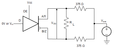
 Figure 21. Measurement of Driver Differential and Common-Mode Output With RS-485 Load
  Figure 22. Measurement of Driver Differential Output Rise and Fall Times and Propagation Delays
  Figure 23. Measurement of Driver Enable and Disable Times With Active High Output and Pull-Down Load
  Figure 24. Measurement of Driver Enable and Disable Times With Active Low Output and Pull-up Load
  Figure 25. Measurement of Receiver Output Rise and Fall Times and Propagation Delays
  Figure 26. Measurement of Receiver Enable/Disable Times With Driver Enabled
  Figure 27. Measurement of Receiver Enable Times With Driver Disabled