JAJSMO1B December 2022 – March 2024 THVD2410V , THVD2412V , THVD2450V , THVD2452V
PRODUCTION DATA
- 1
- 1 特長
- 2 アプリケーション
- 3 概要
- 4 Pin Configuration and Functions
-
5 Specifications
- 5.1 Absolute Maximum Ratings
- 5.2 ESD Ratings
- 5.3 ESD Ratings [IEC]
- 5.4 Recommended Operating Conditions
- 5.5 Thermal Information
- 5.6 Power Dissipation
- 5.7 Electrical Characteristics
- 5.8 Switching Characteristics_250 kbps
- 5.9 Switching Characteristics_1 Mbps
- 5.10 Switching Characteristics_20 Mbps
- 5.11 Switching Characteristics_50 Mbps
- 5.12 Typical Characteristics
- 6 Parameter Measurement Information
- 7 Detailed Description
- 8 Application and Implementation
- 9 Device and Documentation Support
- 10Revision History
- 11Mechanical, Packaging, and Orderable Information
8.2.3 Application Curves
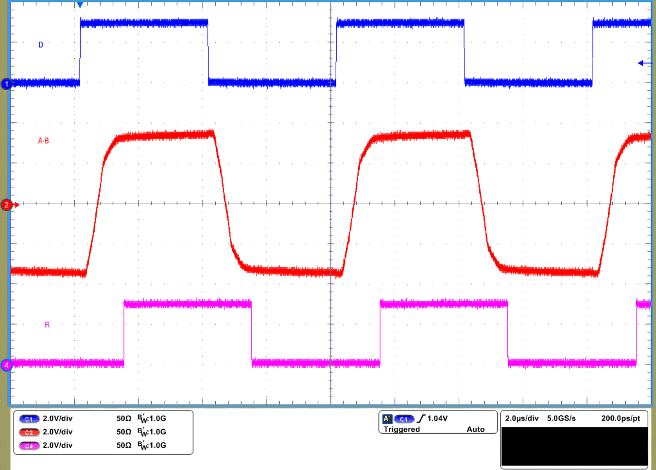
50% duty square wave on D pin
at 250 kbps
Figure 8-8 THVD2410V Waveforms at VCC = 5 V| SLR = VIO | RL = 54 Ω | DE = VIO |
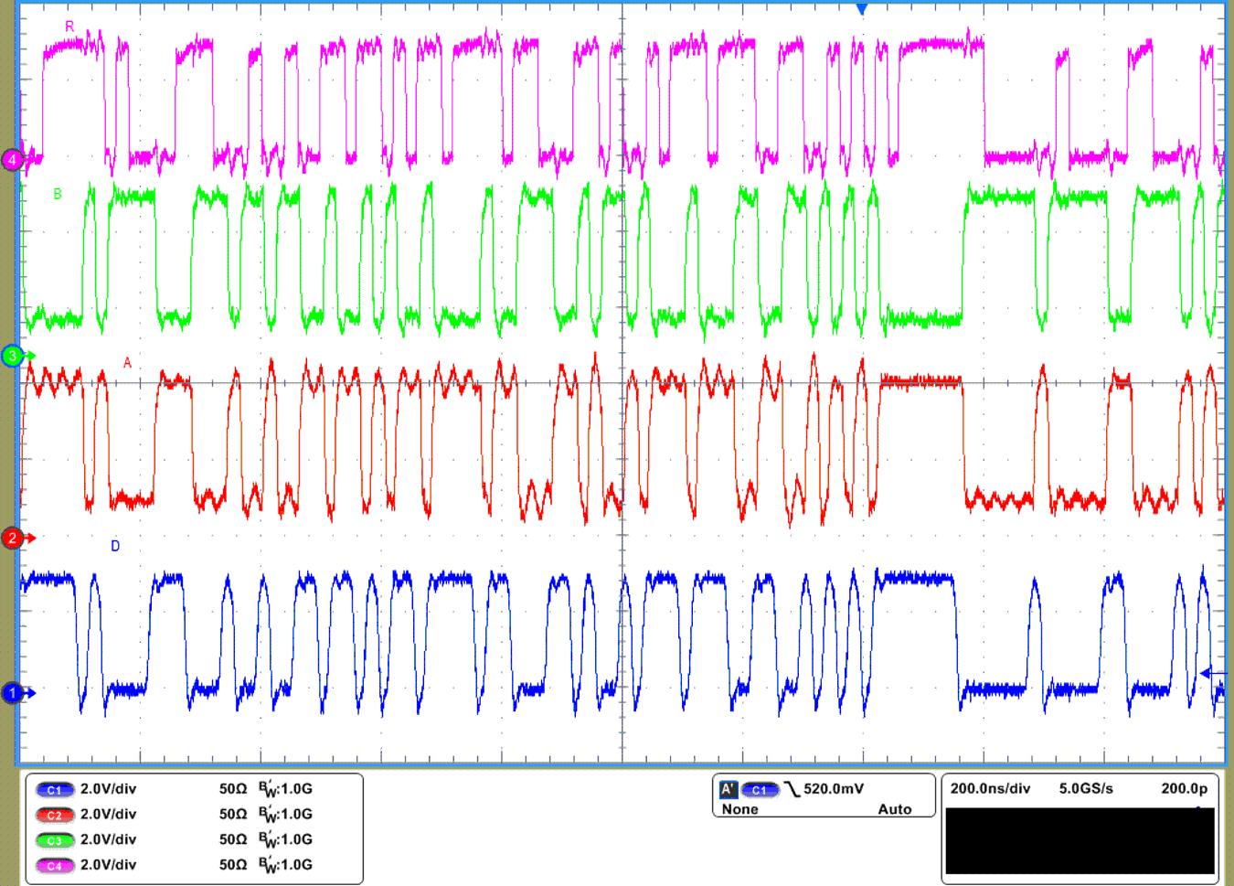
Random
(PRBS7) data on D pin at 50 Mbps
Figure 8-10 THVD2450V Waveforms at VCC = 5 V| SLR = GND | RL = 54 Ω | DE = VIO |
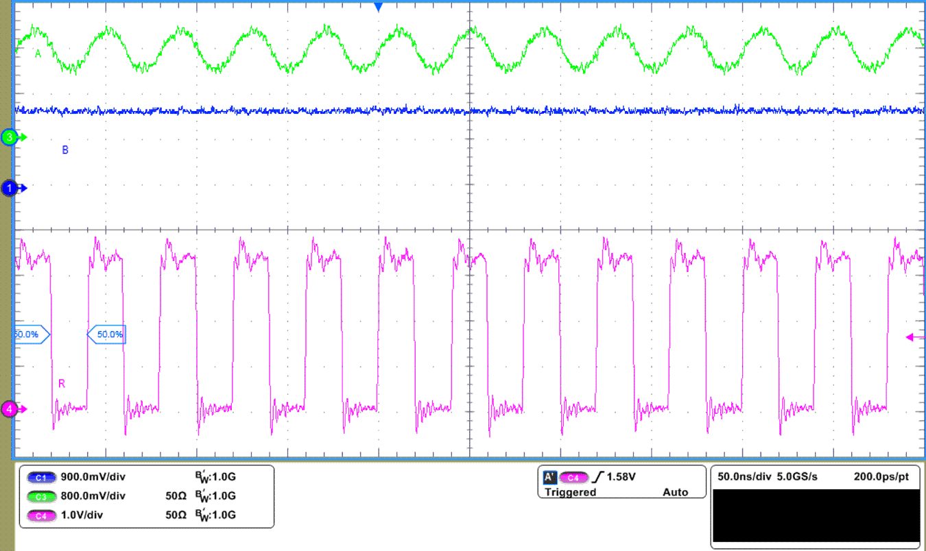
A pin
given ±200mV VID with DC offset of 1.5 V
Figure 8-12 THVD2450V Receiver Waveform with ±200 mV VID| RE = GND | B pin at 1.5 V | |
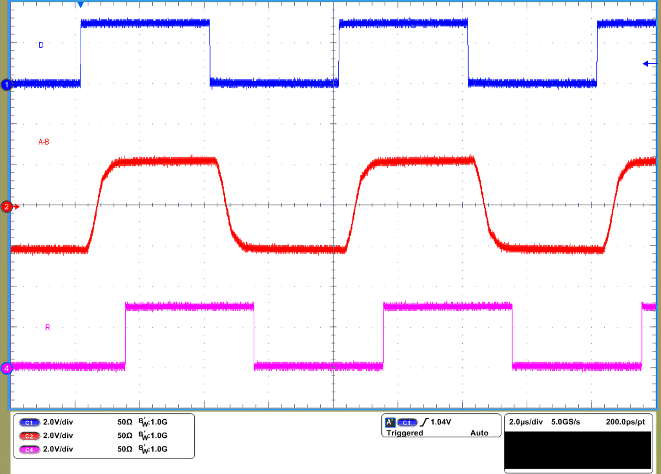
50% duty
square wave on D pin at 250 kbps
Figure 8-9 THVD2410V Waveforms at VCC = 3.3 V| SLR = VIO | RL = 54 Ω | DE = VIO |
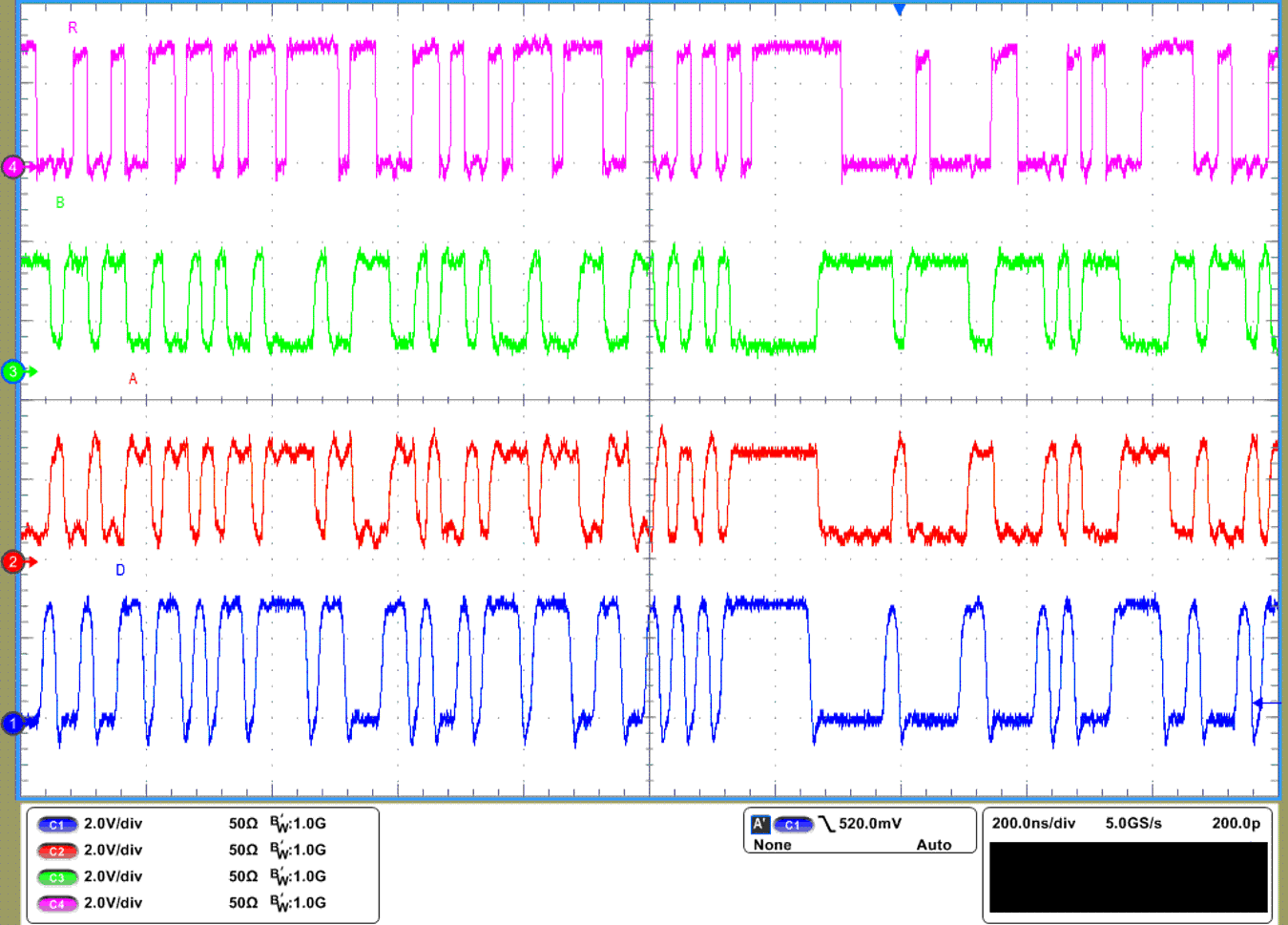
Random
(PRBS7) data on D pin at 50 Mbps
Figure 8-11 THVD2450V Waveforms at VCC = 3.3 V| SLR = GND | RL = 54 Ω | DE = VIO |