JAJSOM2 April   2024 THVD4421

PRODUCTION DATA  

  1.   1
  2. 特長
  3. アプリケーション
  4. 概要
  5. Pin Configuration and Functions
  6. Specifications
    1. 5.1  Absolute Maximum Ratings
    2. 5.2  ESD Ratings
    3. 5.3  ESD Ratings [IEC]
    4. 5.4  Recommended Operating Conditions
    5. 5.5  Thermal Information
    6. 5.6  Power Dissipation
    7. 5.7  Electrical Characteristics
    8. 5.8  Switching Characteristics_RS-485_500kbps
    9. 5.9  Switching Characteristics_RS-485_20Mbps
    10. 5.10 Switching Characteristics, Driver_RS232
    11. 5.11 Switching Characteristics, Receiver_RS232
    12. 5.12 Switching Characteristics_MODE switching
    13. 5.13 Switching Characteristics_RS-485_Termination resistor
    14. 5.14 Switching Characteristics_Loopback mode
    15. 5.15 Typical Characteristics
  7. Parameter Measurement Information
  8. Detailed Description
    1. 7.1 Overview
    2. 7.2 Functional Block Diagrams
    3. 7.3 Feature Description
      1. 7.3.1 Integrated IEC ESD and EFT Protection
      2. 7.3.2 Protection Features
      3. 7.3.3 Receiver Fail-Safe Operation
      4. 7.3.4 Low-Power Shutdown Mode
      5. 7.3.5 On-chip Switchable Termination Resistor
      6. 7.3.6 Operational Data Rate
      7. 7.3.7 Diagnostic Loopback
      8. 7.3.8 Integrated Charge Pump for RS-232
    4. 7.4 Device Functional Modes
      1. 7.4.1 RS-485 Functionality
      2. 7.4.2 RS-232 Functionality
      3. 7.4.3 Mode Control
  9. Application and Implementation
    1. 8.1 Application Information
    2. 8.2 Typical Application
      1. 8.2.1 Design Requirements
        1. 8.2.1.1 Data Rate and Bus Length
        2. 8.2.1.2 Stub Length
        3. 8.2.1.3 Bus Loading
      2. 8.2.2 Detailed Design Procedure
      3. 8.2.3 Application Curves
    3. 8.3 Power Supply Recommendations
    4. 8.4 Layout
      1. 8.4.1 Layout Guidelines
      2. 8.4.2 Layout Example
  10. Device and Documentation Support
    1. 9.1 Device Support
    2. 9.2 ドキュメントの更新通知を受け取る方法
    3. 9.3 サポート・リソース
    4. 9.4 Trademarks
    5. 9.5 静電気放電に関する注意事項
    6. 9.6 用語集
  11. 10Revision History
  12. 11Mechanical, Packaging, and Orderable Information

パッケージ・オプション

メカニカル・データ(パッケージ|ピン)
サーマルパッド・メカニカル・データ
発注情報

Application Curves

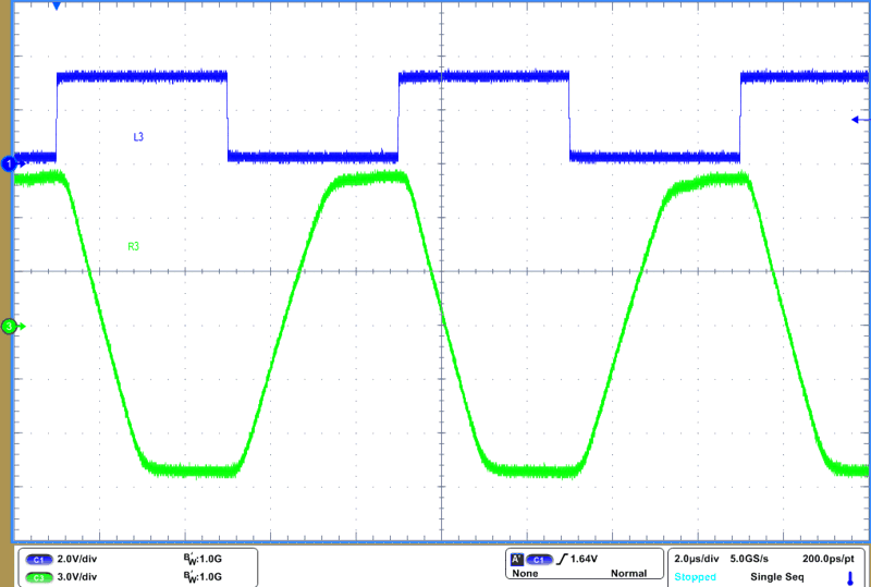
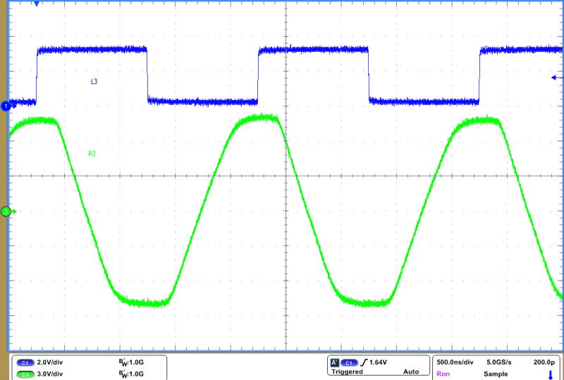
THVD4421 RS-232 Driver Waveform at 250kbps and VCC = 5V
VCC = 5V Bus Load = 5kΩ||2.5nF
250kbps SLR = VIO
Figure 8-5 RS-232 Driver Waveform at 250kbps and VCC = 5V
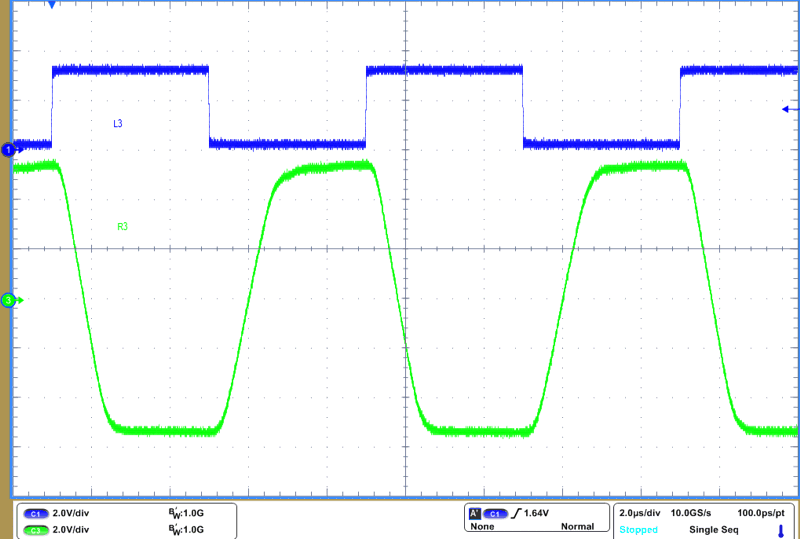
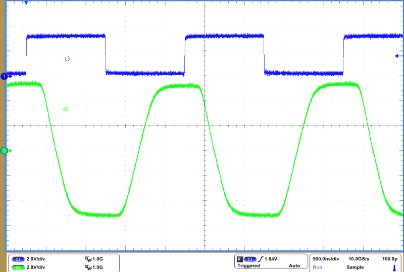
THVD4421 RS-232 Driver Waveform at 250kbps and VCC = 3.3 V
VCC = 3.3V Bus Load = 5kΩ||2.5nF
250kbps SLR = VIO
Figure 8-7 RS-232 Driver Waveform at 250kbps and VCC = 3.3 V
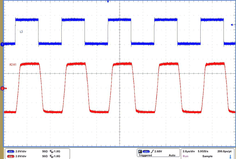
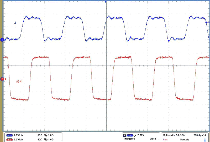
THVD4421 RS-485 Driver Waveform at 500 kbps and VCC = 5 V
VCC = 5V Bus Load = 54Ω||50pF
SLR = VIO Square wave at 500kbps
Figure 8-9 RS-485 Driver Waveform at 500 kbps and VCC = 5 V
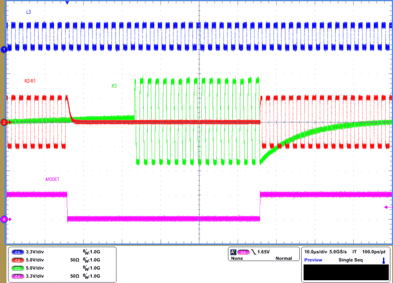
THVD4421 RS-232 to RS-485 Mode Switching Waveform
VCC = 5V L3 = 1 Mbps square wave
SLR = GND MODE1 toggled at 10khz
Figure 8-11 RS-232 to RS-485 Mode Switching Waveform
THVD4421 RS-232 Driver Waveform at 1Mbps and VCC = 5 V
VCC = 5V Bus Load = 5kΩ||1nF
1Mbps SLR = GND
Figure 8-6 RS-232 Driver Waveform at 1Mbps and VCC = 5 V
THVD4421 RS-232 Driver Waveform at 1Mbps and VCC = 3.3 V
VCC = 3.3V RL = 5kΩ||1nF
1kbps SLR = GND
Figure 8-8 RS-232 Driver Waveform at 1Mbps and VCC = 3.3 V
THVD4421 RS-485 Driver Waveform at 20 Mbps and VCC = 5V
VCC = 5V Bus Load = 54Ω||50pF
SLR = GND Square wave at 20kbps
Figure 8-10 RS-485 Driver Waveform at 20 Mbps and VCC = 5V
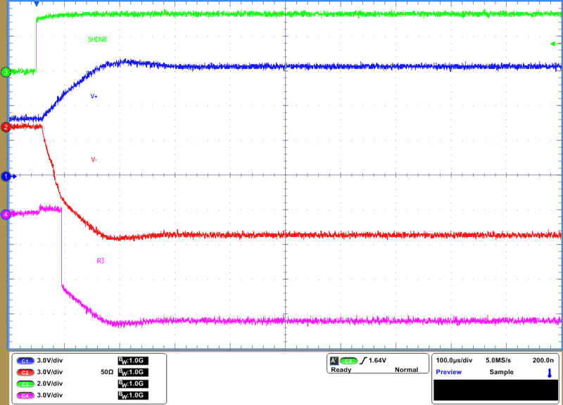
THVD4421 Mode
                        Switching Waveform From Shutdown to RS-232 Mode
VCC = 5V L3 = GND
SHDN toggled
Figure 8-12 Mode Switching Waveform From Shutdown to RS-232 Mode