JAJSJV4 November 2020 THVD8010
PRODUCTION DATA
- 1 特長
- 2 アプリケーション
- 3 概要
- 4 Revision History
- 5 Pin Configuration and Functions
- 6 Specifications
- 7 Parameter Measurement Information
- 8 Detailed Description
- 9 Application and implementation
- 10Power supply recommendations
- 11Layout
- 12Device and Documentation Support
- 13Mechanical, Packaging, and Orderable Information
7 Parameter Measurement Information
Note: The number of pulses shown is reduced for simplicity of waveform. Please see the "OOK
Modulation with F_SET pin" section for more information.
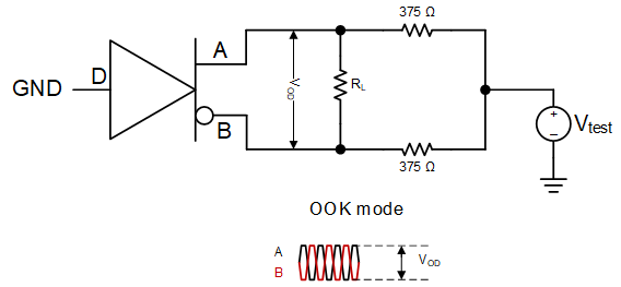 Figure 7-1 Measurement of Driver
Differential Output Voltage With Common-Mode Load
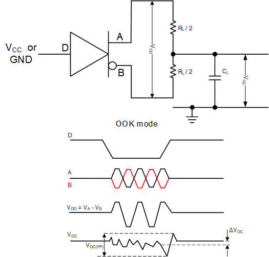 Figure 7-2 Measurement of Driver
Differential and Common-Mode Outputs
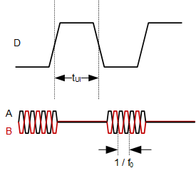 Figure 7-3 Measurement of Carrier
Frequency
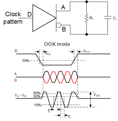 Figure 7-4 Measurement of Driver Switching
Characteristics
Figure 7-5 Measurement of Receiver
Characteristics
Figure 7-6 Transmit to Receive Mode Change with
Low Output
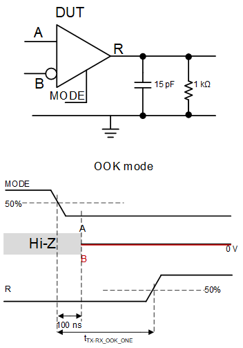 Figure 7-7 Transmit to Receive Mode
Change with High Output
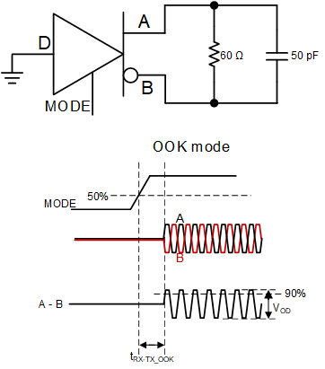 Figure 7-8 Receive to Transmit Mode
Change