JAJSDR6C August   2017  – February 2022 TIC12400-Q1

PRODUCTION DATA  

  1. 特長
  2. アプリケーション
  3. 概要
  4. Revision History
  5. Pin Configuration and Functions
  6. Specifications
    1. 6.1 Absolute Maximum Ratings
    2. 6.2 ESD Ratings
    3. 6.3 Recommended Operating Conditions
    4. 6.4 Thermal Information
    5. 6.5 Electrical Characteristics
    6. 6.6 Timing Requirements
    7. 6.7 Typical Characteristics
  7. Parameter Measurement Information
  8. Detailed Description
    1. 8.1 Overview
    2. 8.2 Functional Block Diagram
    3. 8.3 Feature Description
      1. 8.3.1  VS Pin
      2. 8.3.2  VDD Pin
      3. 8.3.3  Device Initialization
      4. 8.3.4  Device Trigger
      5. 8.3.5  Device Reset
        1. 8.3.5.1 VS Supply POR
        2. 8.3.5.2 Hardware Reset
        3. 8.3.5.3 Software Reset
      6. 8.3.6  VS Under-Voltage (UV) Condition
      7. 8.3.7  VS Over-Voltage (OV) Condition
      8. 8.3.8  Switch Inputs Settings
        1. 8.3.8.1 Input Current Source and Sink Selection
        2. 8.3.8.2 Input Mode Selection
        3. 8.3.8.3 Input Enable Selection
        4. 8.3.8.4 Thresholds Adjustment
        5. 8.3.8.5 Wetting Current Configuration
      9. 8.3.9  Interrupt Generation and INT Assertion
        1. 8.3.9.1 INT Pin Assertion Scheme
        2. 8.3.9.2 Interrupt Idle Time (tINT_IDLE) Time
        3. 8.3.9.3 Microcontroller Wake-Up
        4. 8.3.9.4 Interrupt Enable or Disable and Interrupt Generation Conditions
        5. 8.3.9.5 Detection Filter
      10. 8.3.10 Temperature Monitor
        1. 8.3.10.1 Temperature Warning (TW)
        2. 8.3.10.2 Temperature Shutdown (TSD)
      11. 8.3.11 Parity Check and Parity Generation
      12. 8.3.12 Cyclic Redundancy Check (CRC)
    4. 8.4 Device Functional Modes
      1. 8.4.1 Continuous Mode
      2. 8.4.2 Polling Mode
        1. 8.4.2.1 Standard Polling
        2. 8.4.2.2 Matrix polling
      3. 8.4.3 Additional Features
        1. 8.4.3.1 Clean Current Polling (CCP)
        2. 8.4.3.2 Wetting Current Auto-Scaling
        3. 8.4.3.3 VS Measurement
        4. 8.4.3.4 Wetting Current Diagnostic
        5. 8.4.3.5 ADC Self-Diagnostic
    5. 8.5 Programming
      1. 8.5.1 SPI Communication Interface Buses
        1. 8.5.1.1 Chip Select ( CS)
        2. 8.5.1.2 System Clock (SCLK)
        3. 8.5.1.3 Slave In (SI)
        4. 8.5.1.4 Slave Out (SO)
      2. 8.5.2 SPI Sequence
        1. 8.5.2.1 Read Operation
        2. 8.5.2.2 Write Operation
        3. 8.5.2.3 Status Flag
    6. 8.6 Register Maps
    7. 8.7 Programming Guidelines
  9. Application Information Disclaimer
    1. 9.1 Application Information
    2. 9.2 Using TIC12400-Q1 in a 12 V Automotive System
    3. 9.3 Resistor-coded Switches Detection in Automotive Body Control Module
      1. 9.3.1 Design Requirements
      2. 9.3.2 Detailed Design Procedure
      3. 9.3.3 Application Curves
  10. 10Power Supply Recommendations
  11. 11Layout
    1. 11.1 Layout Guidelines
    2. 11.2 Layout Example
  12. 12Device and Documentation Support
    1. 12.1 Receiving Notification of Documentation Updates
    2. 12.2 サポート・リソース
    3. 12.3 Trademarks
    4. 12.4 Electrostatic Discharge Caution
    5. 12.5 Glossary
  13. 13Mechanical, Packaging, and Orderable Information

パッケージ・オプション

メカニカル・データ(パッケージ|ピン)
サーマルパッド・メカニカル・データ
発注情報

Design Requirements

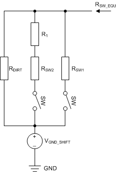
GUID-43FC591D-98E0-46C2-A3AA-AA4BE5387281-low.gifFigure 9-6 Example 3-state Resistor-Coded Switch
Table 9-4 Example Resistor-Coded Switch Specification
SPECIFICATIONMINMAX
VBAT9 V ≤ VBAT ≤ 16 V9 V16 V
R1680 Ω ± 8%625.6 Ω734.4 Ω
RSW150 Ω Max when closed0 Ω50 Ω
RSW250 Ω Max when closed0 Ω50 Ω
RDIRT5000 Ω Min5000 Ω
VGND_SHIFT±1 V-1 Ω+1 Ω

An example of a 3-state resistor-coded switch is shown in Figure 9-6, with Table 9-4 summarizing its detailed specification. The goal of this design is to utilize the TIC12400-Q1’s integrated ADC to detect and differentiate the 3 switch states:

  1. State 1: Both SW1 and SW2 open.
  2. State 2: SW1 open and SW2 close.
  3. State 3: SW1 close and SW2 open.
To mimic real automotive systems, the battery is assumed to be fluctuating between 9 V and 16 V. RDIRT is introduced to model the small leakage flowing across the switch in open state. There is also a ±1 V ground shift present in the system, meaning there could be up to ±1 V of potential difference between the switch reference point and the ground reference of the TIC12400-Q1. When the switch changes position and the switch state changes from one to another, the TIC12400-Q1 is required to correctly detect the state transition and issue an interrupt to alert the microcontroller. The switch information needs to be stored in the status registers for the microcontroller to retrieve.