JAJSVB5A September 2024 – December 2024 TIOL221
PRODMIX
- 1
- 1 特長
- 2 アプリケーション
- 3 概要
- 4 Pin Configuration and Functions
- 5 Specifications
- 6 Parameter Measurement Information
-
7 Detailed Description
- 7.1 Overview
- 7.2 Functional Block Diagrams
- 7.3
Feature Description
- 7.3.1 Wake-Up Detection
- 7.3.2 Current Limit Configuration
- 7.3.3 CQ Current Fault Detection, Indication and Auto Recovery
- 7.3.4 DO Current Fault Detection, Indication and Auto Recovery
- 7.3.5 CQ and DI Receivers
- 7.3.6 Fault Reporting
- 7.3.7 The Integrated Voltage Regulator (LDO)
- 7.3.8 Reverse Polarity Protection
- 7.3.9 Integrated Surge Protection and Transient Waveform Tolerance
- 7.3.10 Undervoltage Lock-Out (UVLO)
- 7.3.11 Interrupt Function
- 7.4 Device Functional Modes
- 7.5 SPI Programming
- 8 Application and Implementation
- 9 TIOL221 Registers
- 10Device and Documentation Support
- 11Revision History
- 12Mechanical, Packaging, and Orderable Information
パッケージ・オプション
デバイスごとのパッケージ図は、PDF版データシートをご参照ください。
メカニカル・データ(パッケージ|ピン)
- RGE|24
サーマルパッド・メカニカル・データ
発注情報
6 Parameter Measurement Information
 Figure 6-1 Test Circuit for Driver Switching
 Figure 6-2 Waveforms for Driver Output Switching Measurements
 Figure 6-3 Waveforms for Driver Enable or Disable Time Measurements
 Figure 6-4 Test Circuit for Receiver Switching
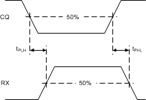
 Figure 6-5 Receiver Switching Measurements
 Figure 6-6 Overcurrent and Wake Conditions for EN = H and ILIM_ADJ = 10kΩ to 110kΩ,
TX = H (Full Lines); and TX = L (Red Dotted Lines)
 Figure 6-7 Overcurrent and Wake Conditions for EN = H and ILIM_ADJ is floating, TX = H (Full Lines); and TX = L (Red Dotted Lines)
 Figure 6-8 SPI Read/Write Timing Characteristics
 Figure 6-9 Driving the Inductive Load
 Figure 6-10 Driving the Capacitive Load
 Figure 6-11 Interrupt Pin Toggling Behavior (SPI Mode; INT_TOG = 1b)