JAJSLT3N november 1978 – august 2023 TL061 , TL061A , TL061B , TL062 , TL062A , TL062B , TL064 , TL064A , TL064B
PRODUCTION DATA
- 1
- 1 特長
- 2 アプリケーション
- 3 概要
- 4 Revision History
- 5 Pin Configuration and Functions
-
6 Specifications
- 6.1 Absolute Maximum Ratings
- 6.2 ESD Ratings
- 6.3 Recommended Operating Conditions
- 6.4 Thermal Information (TL061)
- 6.5 Thermal Information (TL062)
- 6.6 Thermal Information (TL064)
- 6.7 Electrical Characteristics for TL06xC and TL06xxC
- 6.8 Electrical Characteristics for TL06xxC and TL06xI
- 6.9 Electrical Characteristics for TL06xM
- 6.10 Operating Characteristics
- Typical Characteristics
- 7 Parameter Measurement Information
- 8 Detailed Description
- 9 Applications and Implementation
- 10Device and Documentation Support
- 11Mechanical, Packaging, and Orderable Information
パッケージ・オプション
デバイスごとのパッケージ図は、PDF版データシートをご参照ください。
メカニカル・データ(パッケージ|ピン)
- D|8
- P|8
- PS|8
- PW|8
サーマルパッド・メカニカル・データ
- PS|8
発注情報
Typical Characteristics
Data at high and low temperatures are applicable only within the specified operating free-air temperature ranges of the various devices.
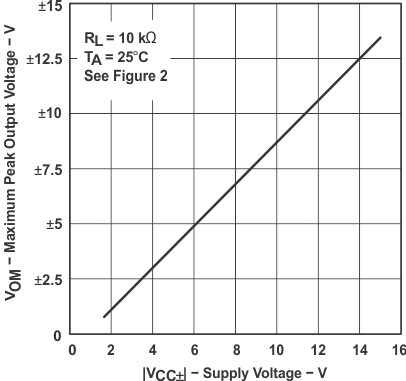 Figure 6-1 Maximum Peak Output Voltage vs Supply Voltage
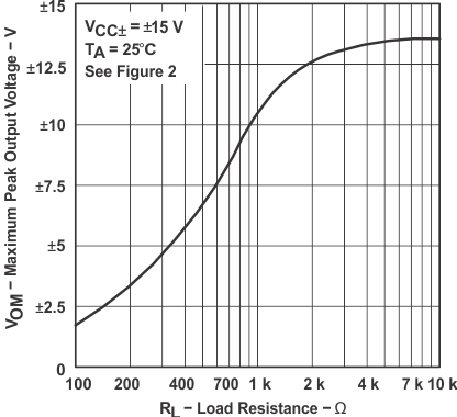 Figure 6-3 Maximum Peak Output Voltage vs Load Resistance
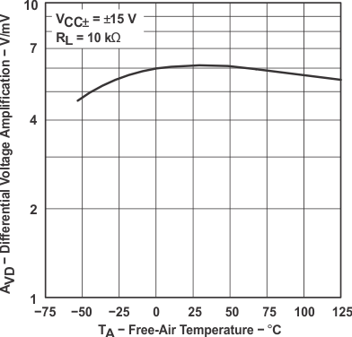 Figure 6-5 Differential Voltage Amplification vs Free-Air Temperature
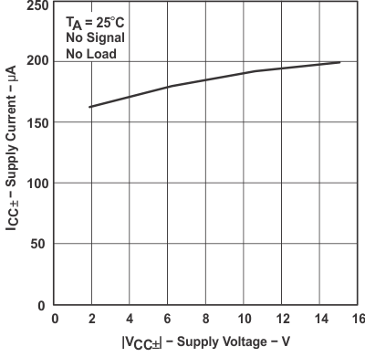 Figure 6-7 Supply Current vs Supply Voltage
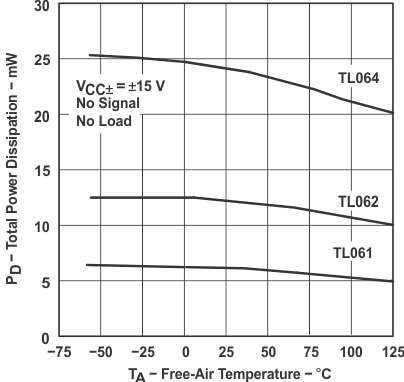 Figure 6-9 Total Power Dissipation vs Free-Air Temperature
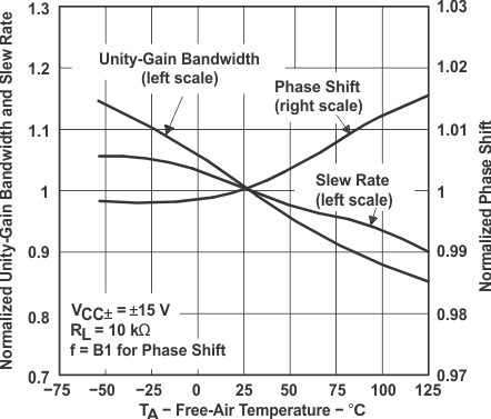 Figure 6-11 Normalized Unity-Gain Bandwidth, Slew Rate, and Phase Shift vs Free-Air Temperature
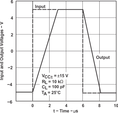 Figure 6-13 Voltage-Follower Large-Signal Pulse Response vs Time
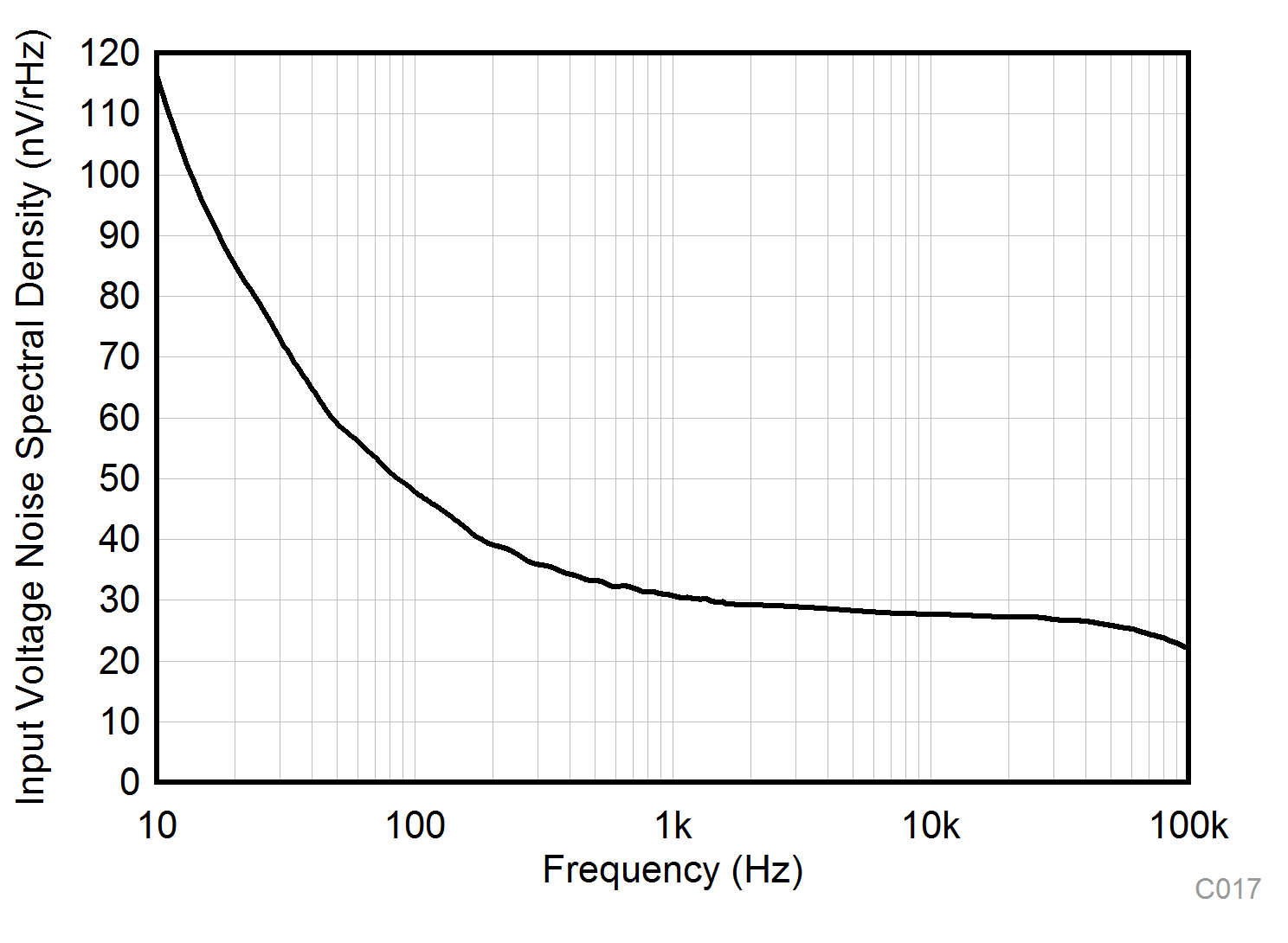 Figure 6-15 Equivalent Input Noise Voltage vs Frequency
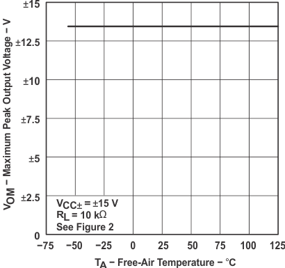 Figure 6-2 Maximum Peak Output Voltage vs Free-Air Temperature
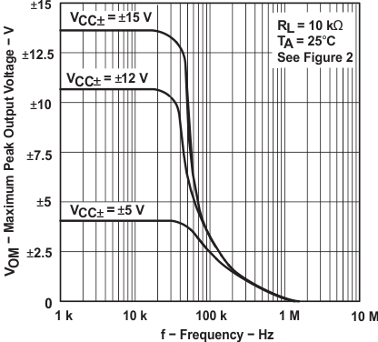 Figure 6-4 Maximum Peak Output Voltage vs Frequency
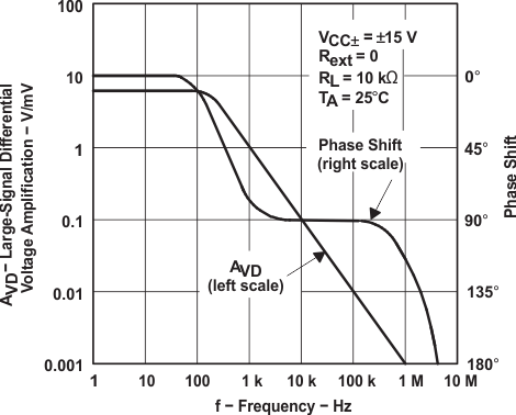 Figure 6-6 Large-Signal Differential Voltage Amplification and Phase Shift vs Frequency
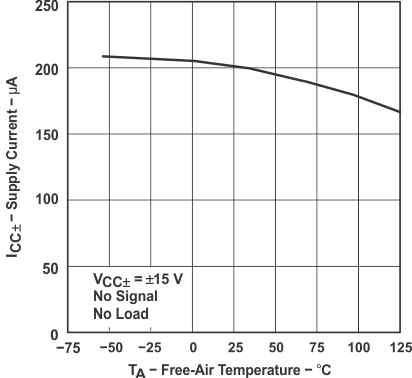 Figure 6-8 Supply Current vs Free-Air Temperature
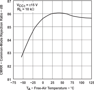 Figure 6-10 All Except TL06_C Common-Mode Rejection Ratio vs Free-Air Temperature
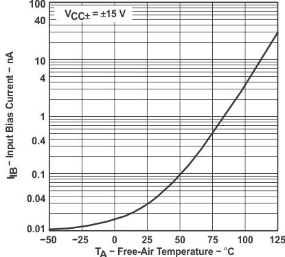 Figure 6-12 Input Bias Current vs Free-Air Temperature
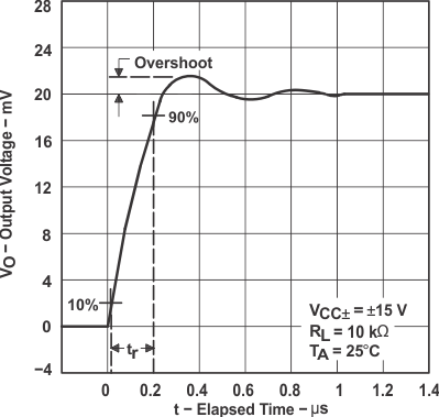 Figure 6-14 Output Voltage vs Elapsed Time