JAJSI95 December 2019 TL16C750E
PRODUCTION DATA.
- 1 特長
- 2 アプリケーション
- 3 概要
- 4 改訂履歴
- 5 概要 (続き)
- 6 Pin Configuration and Functions
- 7 Specifications
- 8 Parameter Measurement Information
-
9 Detailed Description
- 9.1 Overview
- 9.2 Functional Block Diagrams
- 9.3
Feature Description
- 9.3.1 UART Modes
- 9.3.2 Trigger Levels
- 9.3.3 Hardware Flow Control
- 9.3.4 Auto-RTS
- 9.3.5 Auto-CTS
- 9.3.6 Software Flow Control
- 9.3.7 Software Flow Control Example
- 9.3.8 Reset
- 9.3.9 Interrupts
- 9.3.10 Interrupt Mode Operation
- 9.3.11 Polled Mode Operation
- 9.3.12 Break and Timeout Conditions
- 9.3.13 Programmable Baud Rate Generator with Fractional Divisor
- 9.3.14 Fractional Divisor
- 9.4 Device Functional Modes
- 9.5
Register Maps
- 9.5.1 Registers Operations
- 9.5.2 Receiver Holding Register (RHR)
- 9.5.3 Transmit Holding Register (THR)
- 9.5.4 FIFO Control Register (FCR)
- 9.5.5 Line Control Register (LCR)
- 9.5.6 Line Status Register (LSR)
- 9.5.7 Modem Control Register (MCR)
- 9.5.8 Modem Status Register (MSR)
- 9.5.9 Interrupt Enable Register (IER)
- 9.5.10 Interrupt Identification Register (IIR)
- 9.5.11 Enhanced Feature Register (EFR)
- 9.5.12 Divisor Latches (DLL, DLH, DLF)
- 9.5.13 Transmission Control Register (TCR)
- 9.5.14 Trigger Level Register (TLR)
- 9.5.15 FIFO Ready Register
- 9.5.16 Alternate Function Register (AFR)
- 9.5.17 RS-485 Mode
- 9.5.18 IrDA Overview
- 9.5.19 IrDA Encoder Function
- 10Application and Implementation
- 11Power Supply Recommendations
- 12Layout
- 13デバイスおよびドキュメントのサポート
- 14メカニカル、パッケージ、および注文情報
9.3.6 Software Flow Control
Software flow control is enabled through the enhanced feature register and the modem control register. Different combinations of software flow control can be enabled by setting different combinations of EFR[3−0]. Table 6 shows software flow control options.
Two other enhanced features relate to software flow control:
- Xon Any Function [MCR(5): Operation resumes after receiving any character after recognizing the Xoff character.
- Special Character [EFR(5)]: Incoming data is compared to Xoff2. Detection of the special character sets the Xoff interrupt [IIR(4)] but does not halt transmission. The Xoff interrupt is cleared by a read of the IIR. The special character is transferred to the RX FIFO.
NOTE
It is possible for an Xon1 character to be recognized as an Xon Any character, which could cause an Xon2 character to be written to the RX FIFO.
Table 6. Software Flow Control Options EFR[3:0]
| BIT 3 | BIT 2 | BIT 1 | BIT 0 | TX, RX SOFTWARE FLOW CONTROLS |
|---|---|---|---|---|
| 0 | 0 | X | X | No transmit flow control |
| 1 | 0 | X | X | Transmit Xon1, Xoff1 |
| 0 | 1 | X | X | Transmit Xon2, Xoff2 |
| 1 | 1 | X | X | Transmit Xon1, Xon2: Xoff1, Xoff2 |
| X | X | 0 | 0 | No receive flow control |
| X | X | 1 | 0 | Receiver compares Xon1, Xoff1 |
| X | X | 0 | 1 | Receiver compares Xon2, Xoff2 |
| 1 | 0 | 1 | 1 | Transmit Xon1, Xoff1
Receiver compares Xon1 or Xon2, Xoff1 or Xoff2 |
| 0 | 1 | 1 | 1 | Transmit Xon2, Xoff2
Receiver compares Xon1 or Xon2, Xoff1 or Xoff2 |
| 1 | 1 | 1 | 1 | Transmit Xon1, Xon2: Xoff1, Xoff2
Receiver compares Xon1 and Xon2: Xoff1 and Xoff2 |
| 0 | 0 | 1 | 1 | No transmit flow control
Receiver compares Xon1 and Xon2: Xoff1 and Xoff2 |
When software flow control operation is enabled, the TL16C750E device compares incoming data with Xoff1 and Xoff2 programmed characters (in certain cases Xoff1 and Xoff2 must be received sequentially). (1) When an Xoff character is received, transmission is halted after completing transmission of the current character. Xoff character detection also sets IIR[4] and causes INT to go high (if enabled via IER[5]).
To resume transmission an Xon1 and Xon2 character must be received (in certain cases Xon1 and Xon2 must be received sequentially). When the correct Xon characters are received IIR[4] is cleared and the Xoff interrupt disappears.
NOTE
If a parity, framing, or break error occurs while receiving a software flow control character, this character is treated as normal data and is written to the RCV FIFO.
Xoff1 and Xoff2 characters are transmitted when the RX FIFO has passed the programmed trigger level TCR[3:0].
Xon1 and Xon2 characters are transmitted when the RX FIFO reaches the trigger level programmed via TCR[7:4].
NOTE
If, after an Xoff character has been sent, software flow control is disabled, the UART transmits Xon characters automatically to enable normal transmission to proceed. A feature of the TL16C750E UART design is that if the software flow combination (EFR[3:0]) changes after an Xoff has been sent, the originally programmed Xon is automatically sent. If the RX FIFO is still above the trigger level, the newly programmed Xoff1 or Xoff2 is transmitted.
The transmission of Xoff and Xon follows the exact same protocol as transmission of an ordinary byte from the FIFO. This means that even if the word length is set to be 5, 6, or 7 characters, then the 5, 6, or 7 least significant bits of Xoff1, Xoff2 and Xon1, Xon2 are transmitted. The transmission of 5, 6, or 7 bits of a character is seldom done, but this functionality is included to maintain compatibility with earlier designs.
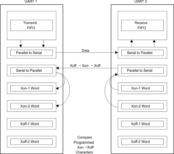
It is assumed that software flow control and hardware flow control are never enabled simultaneously. Figure 23 shows a software flow control example.
 Figure 23. Software Flow Control Example