SLVS641B April 2008 – March 2015 TL4242
PRODUCTION DATA.
- 1 Features
- 2 Applications
- 3 Description
- 4 Revision History
- 5 Pin Configuration and Functions
- 6 Specifications
- 7 Detailed Description
- 8 Application and Implementation
- 9 Power Supply Recommendations
- 10Layout
- 11Device and Documentation Support
- 12Mechanical, Packaging, and Orderable Information
パッケージ・オプション
メカニカル・データ(パッケージ|ピン)
- DRJ|8
サーマルパッド・メカニカル・データ
- DRJ|8
発注情報
8 Application and Implementation
NOTE
Information in the following applications sections is not part of the TI component specification, and TI does not warrant its accuracy or completeness. TI’s customers are responsible for determining suitability of components for their purposes. Customers should validate and test their design implementation to confirm system functionality.
8.1 Application Information
8.1.1 Input Supply Voltage
The input supply voltage calculates as the sum of the LED forward voltages, the TL4242 drop voltage, and the voltage drop across the shunt resistor, RREF. The total LED forward voltage depends on the type of LED and the number of LEDs in the string. The TL4242 drop voltage must be greater than Vdr (typically 350 mV), but must not be too high as this could cause excessive power dissipation inside the device. The voltage drop across the shunt resistor is typically 177 mV.
8.1.2 Power Dissipation in TL4242
Power dissipation in the TL4242 will come from two sources:
- Quiescent power: (Input voltage × Supply current)
- Power dissipation in the pass element:
The power dissipation in the pass element can be significant if the input voltage, VI, is much higher than VQ. The power dissipation is also dependent on the LED current. Equation 4 is an example calculation using the design parameters listed in Table 2.
Table 2. Design Parameters
| DESIGN PARAMETER | EXAMPLE VALUE | |||
|---|---|---|---|---|
| VI | 13.5 V | |||
| VQ | 7 V | |||
| IQ | 0.2 A | |||
In Equation 4, there is 1.3 W of power dissipation in the pass element of the TL4242. This power dissipation will cause the junction temperature of the device to increase. The increase in temperature is equal to RθJA × 1.3 W. Please note that RθJA is dependent on the PCB layout.
8.1.3 Setting the Output Current
An external shunt resistor in the ground path of the connected LEDs is used to sense the LED current. A regulation loop holds the voltage drop at the shunt resistor at a constant level of 177 mV (typical). The constant-current level can be adjusted by selecting the shunt resistance, RREF. Calculate the typical output current using the equation:
where
- VREF is the reference voltage (typically 177 mV) (see Electrical Characteristics).
The equation applies for RREF = 0.39 Ω to 10 Ω.
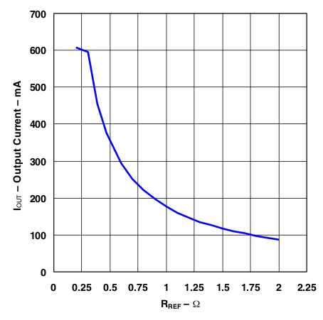
The output current is shown as a function of the reference resistance in Figure 1.
8.2 Typical Application
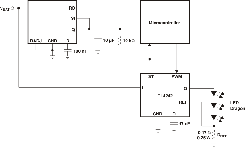
Figure 6 shows a typical application with the TL4242 driving three LEDs in series.
 Figure 6. Application Circuit
8.2.1 Design Requirements
For this design example, use the following as the input parameters in Table 3.
Table 3. Design Parameters
| DESIGN PARAMETERS | EXAMPLE VALUE | |||
|---|---|---|---|---|
| # of LEDs | 3 | |||
| Forward Voltage of each LED | 3.5 V | |||
| LED Current | 377 mA | |||
8.2.2 Detailed Design Procedure
8.2.2.1 Input Voltage
The input voltage must be greater than the sum of the LED forward voltages, the TL4242 drop voltage, and the voltage drop across the shunt resistor, RREF. In this design example, the total LED forward voltage is 3 × 3.5 V = 10.5 V. The typical TL4242 drop voltage is 350 mV. The typical voltage drop across the shunt resistor is 177 mV. In sum, the input voltage must be greater than 10.5 + 0.350 + 0.177 = 11.027 V. An appropriate input voltage for this application would be 12 V.
8.2.2.2 Shunt Resistor
The shunt resistor value, RREF, can be calculated based on the desired LED current.
where
- VREF is the reference voltage (typically 177 mV) (see Electrical Characteristics).
As shown in Design Requirements, the desired LED current is 377 mA. The appropriate RREF value for this application calculates to be 0.47 Ω.
8.2.3 Application Curve
 Figure 7. Output Current vs External Resistor