SLVS641B April 2008 – March 2015 TL4242
PRODUCTION DATA.
- 1 Features
- 2 Applications
- 3 Description
- 4 Revision History
- 5 Pin Configuration and Functions
- 6 Specifications
- 7 Detailed Description
- 8 Application and Implementation
- 9 Power Supply Recommendations
- 10Layout
- 11Device and Documentation Support
- 12Mechanical, Packaging, and Orderable Information
パッケージ・オプション
メカニカル・データ(パッケージ|ピン)
- DRJ|8
サーマルパッド・メカニカル・データ
- DRJ|8
発注情報
10 Layout
10.1 Layout Guidelines
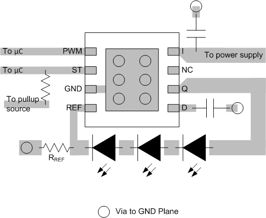
The REF pin should be routed directly to the shunt resistor, RREF. If there is a long PCB trace between the LED string and the shunt resistor, the REF pin should connect close to the shunt resistor (rather than close to the LED string) to allow for accurate sensing across the shunt resistor.
The traces for I and Q will carry the full LED current. These traces should be the appropriate width to carry the LED current.
The exposed thermal pad on the bottom of the TL4242 should be connected to the PCB. The thermal pad helps to dissipate heat in the case of high power dissipation in the device. To further enhance the thermal performance of the device, the thermal pad can be connected by vias to the ground layer in the PCB.
10.2 Layout Example
 Figure 8. PCB Layout