JAJSHC3A May   2019  – November 2019 TL431LI-Q1 , TL432LI-Q1

PRODUCTION DATA.  

  1. 特長
  2. アプリケーション
  3. 概要
    1.     Device Images
      1.      概略回路図
  4. 改訂履歴
  5. Device Comparison Table
  6. Pin Configuration and Functions
    1.     Pin Functions
  7. Specifications
    1. 7.1 Absolute Maximum Ratings
    2. 7.2 ESD Ratings
    3. 7.3 Recommended Operating Conditions
    4. 7.4 Thermal Information
    5. 7.5 Electrical Characteristics
    6. 7.6 Typical Characteristics
  8. Parameter Measurement Information
    1. 8.1 Temperature Coefficient
    2. 8.2 Dynamic Impedance
  9. Detailed Description
    1. 9.1 Overview
    2. 9.2 Functional Block Diagram
    3. 9.3 Feature Description
    4. 9.4 Device Functional Modes
      1. 9.4.1 Open Loop (Comparator)
      2. 9.4.2 Closed Loop
  10. 10Applications and Implementation
    1. 10.1 Application Information
    2. 10.2 Typical Applications
      1. 10.2.1 Comparator With Integrated Reference
      2. 10.2.2 Design Requirements
      3. 10.2.3 Detailed Design Procedure
        1. 10.2.3.1 Basic Operation
          1. 10.2.3.1.1 Overdrive
        2. 10.2.3.2 Output Voltage and Logic Input Level
          1. 10.2.3.2.1 Input Resistance
      4. 10.2.4 Application Curves
      5. 10.2.5 Precision LED Lighting Current Sink Regulator
        1. 10.2.5.1 Design Requirements
        2. 10.2.5.2 Detailed Design Procedure
          1. 10.2.5.2.1 Basic Operation
            1. 10.2.5.2.1.1 Output Current Range and Accuracy
          2. 10.2.5.2.2 Power Consumption
      6. 10.2.6 Shunt Regulator/Reference
        1. 10.2.6.1 Design Requirements
        2. 10.2.6.2 Detailed Design Procedure
          1. 10.2.6.2.1 Programming Output/Cathode Voltage
          2. 10.2.6.2.2 Total Accuracy
          3. 10.2.6.2.3 Stability
          4. 10.2.6.2.4 Start-up Time
        3. 10.2.6.3 Application Curves
      7. 10.2.7 Isolated Flyback with Optocoupler
        1. 10.2.7.1 Design Requirements
        2. 10.2.7.2 Detailed Design Procedure
          1. 10.2.7.2.1 TL431 Feedback Loop Error Calculation
    3. 10.3 System Examples
  11. 11Power Supply Recommendations
  12. 12Layout
    1. 12.1 Layout Guidelines
    2. 12.2 Layout Example
  13. 13デバイスおよびドキュメントのサポート
    1. 13.1 デバイス・サポート
      1. 13.1.1 デバイスの項目表記
    2. 13.2 ドキュメントのサポート
      1. 13.2.1 関連資料
    3. 13.3 関連リンク
    4. 13.4 ドキュメントの更新通知を受け取る方法
    5. 13.5 サポート・リソース
    6. 13.6 商標
    7. 13.7 静電気放電に関する注意事項
    8. 13.8 Glossary
  14. 14メカニカル、パッケージ、および注文情報

パッケージ・オプション

メカニカル・データ(パッケージ|ピン)
サーマルパッド・メカニカル・データ
発注情報

System Examples

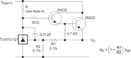
TL431LI-Q1 TL432LI-Q1 ai_prec_hi_curr_ser_slvsdq6.gif
R should provide cathode current ≥0.6 mA to the TL431LI-Q1 at minimum V(BATT).
Figure 27. Precision High-Current Series Regulator
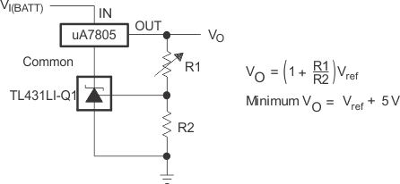
TL431LI-Q1 TL432LI-Q1 ai_out_ctrl_3term_slvsdq6.gifFigure 28. Output Control of a Three-Terminal Fixed Regulator
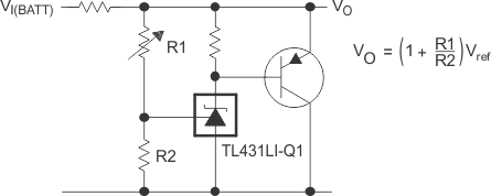
TL431LI-Q1 TL432LI-Q1 ai_high_curr_shunt_slvsdq6.gifFigure 29. High-Current Shunt Regulator
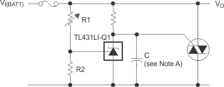
TL431LI-Q1 TL432LI-Q1 ai_crowbar_slvsdq6.gif
Refer to the stability boundary conditions in Figure 12 to determine allowable values for C.
Figure 30. Crowbar Circuit
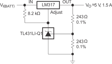
TL431LI-Q1 TL432LI-Q1 ai_prec_5v_1p5a_reg_slvsdq6.gifFigure 31. Precision 5-V, 1.5-A Regulator
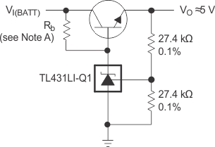
TL431LI-Q1 TL432LI-Q1 ai_efficient_5v_slvsdq6.gif
Rb should provide cathode current ≥0.6 mA to the TL431LI-Q1.
Figure 32. Efficient 5-V Low-Dropout (LDO) Regulator Configuration
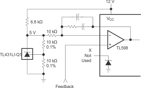
TL431LI-Q1 TL432LI-Q1 ai_pwm_conv_slvsdq6.gifFigure 33. PWM Converter With Reference
TL431LI-Q1 TL432LI-Q1 ai_voltage_monitor_slvsdq6.gif
Select R3 and R4 to provide the desired LED intensity and cathode current ≥0.6 mA to the TL431LI-Q1 at the available VI(BATT).
Figure 34. Voltage Monitor
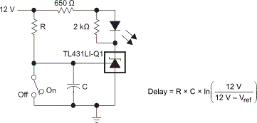
TL431LI-Q1 TL432LI-Q1 ai_delay_timer_slvsdq6.gifFigure 35. Delay Timer
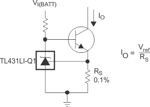
TL431LI-Q1 TL432LI-Q1 ai_prec_curr_limit_slvsdq6.gifFigure 36. Precision Current Limiter
TL431LI-Q1 TL432LI-Q1 ai_prec_const_curr_slvsdq6.gifFigure 37. Precision Constant-Current Sink