JAJSHL0A June   2019  – December 2019 TLA2518

PRODUCTION DATA.  

  1. 特長
  2. アプリケーション
  3. 概要
    1.     Device Images
      1.      TLA2518 のブロック図とアプリケーション
  4. 改訂履歴
  5. Pin Configuration and Functions
    1.     Pin Functions
  6. Specifications
    1. 6.1 Absolute Maximum Ratings
    2. 6.2 ESD Ratings
    3. 6.3 Recommended Operating Conditions
    4. 6.4 Thermal Information
    5. 6.5 Electrical Characteristics
    6. 6.6 Timing Requirements
    7. 6.7 Switching Characteristics
    8. 6.8 Typical Characteristics
  7. Detailed Description
    1. 7.1 Overview
    2. 7.2 Functional Block Diagram
    3. 7.3 Feature Description
      1. 7.3.1 Multiplexer and ADC
      2. 7.3.2 Reference
      3. 7.3.3 ADC Transfer Function
      4. 7.3.4 ADC Offset Calibration
      5. 7.3.5 Programmable Averaging Filter
      6. 7.3.6 General-Purpose I/Os
      7. 7.3.7 Oscillator and Timing Control
      8. 7.3.8 Output Data Format
      9. 7.3.9 Device Programming
        1. 7.3.9.1 Enhanced-SPI Interface
        2. 7.3.9.2 Register Read/Write Operation
          1. 7.3.9.2.1 Register Write
          2. 7.3.9.2.2 Register Read
    4. 7.4 Device Functional Modes
      1. 7.4.1 Device Power-Up and Reset
      2. 7.4.2 Manual Mode
      3. 7.4.3 On-the-Fly Mode
      4. 7.4.4 Auto-Sequence Mode
    5. 7.5 TLA2518 Registers
      1. 7.5.1  SYSTEM_STATUS Register (Address = 0x0) [reset = 0x81]
        1. Table 9. SYSTEM_STATUS Register Field Descriptions
      2. 7.5.2  GENERAL_CFG Register (Address = 0x1) [reset = 0x0]
        1. Table 10. GENERAL_CFG Register Field Descriptions
      3. 7.5.3  DATA_CFG Register (Address = 0x2) [reset = 0x0]
        1. Table 11. DATA_CFG Register Field Descriptions
      4. 7.5.4  OSR_CFG Register (Address = 0x3) [reset = 0x0]
        1. Table 12. OSR_CFG Register Field Descriptions
      5. 7.5.5  OPMODE_CFG Register (Address = 0x4) [reset = 0x0]
        1. Table 13. OPMODE_CFG Register Field Descriptions
      6. 7.5.6  PIN_CFG Register (Address = 0x5) [reset = 0x0]
        1. Table 14. PIN_CFG Register Field Descriptions
      7. 7.5.7  GPIO_CFG Register (Address = 0x7) [reset = 0x0]
        1. Table 15. GPIO_CFG Register Field Descriptions
      8. 7.5.8  GPO_DRIVE_CFG Register (Address = 0x9) [reset = 0x0]
        1. Table 16. GPO_DRIVE_CFG Register Field Descriptions
      9. 7.5.9  GPO_VALUE Register (Address = 0xB) [reset = 0x0]
        1. Table 17. GPO_VALUE Register Field Descriptions
      10. 7.5.10 GPI_VALUE Register (Address = 0xD) [reset = 0x0]
        1. Table 18. GPI_VALUE Register Field Descriptions
      11. 7.5.11 SEQUENCE_CFG Register (Address = 0x10) [reset = 0x0]
        1. Table 19. SEQUENCE_CFG Register Field Descriptions
      12. 7.5.12 CHANNEL_SEL Register (Address = 0x11) [reset = 0x0]
        1. Table 20. CHANNEL_SEL Register Field Descriptions
      13. 7.5.13 AUTO_SEQ_CH_SEL Register (Address = 0x12) [reset = 0x0]
        1. Table 21. AUTO_SEQ_CH_SEL Register Field Descriptions
  8. Application and Implementation
    1. 8.1 Application Information
    2. 8.2 Typical Applications
      1. 8.2.1 Mixed-Channel Configuration
        1. 8.2.1.1 Design Requirements
        2. 8.2.1.2 Detailed Design Procedure
          1. 8.2.1.2.1 Digital Input
          2. 8.2.1.2.2 Digital Open-Drain Output
          3. 8.2.1.2.3 Application Curve
      2. 8.2.2 Digital Push-Pull Output Configuration
  9. Power Supply Recommendations
    1. 9.1 AVDD and DVDD Supply Recommendations
  10. 10Layout
    1. 10.1 Layout Guidelines
    2. 10.2 Layout Example
  11. 11デバイスおよびドキュメントのサポート
    1. 11.1 ドキュメントの更新通知を受け取る方法
    2. 11.2 コミュニティ・リソース
    3. 11.3 商標
    4. 11.4 静電気放電に関する注意事項
    5. 11.5 Glossary
  12. 12メカニカル、パッケージ、および注文情報

パッケージ・オプション

メカニカル・データ(パッケージ|ピン)
サーマルパッド・メカニカル・データ
発注情報

Enhanced-SPI Interface

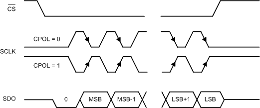
The device features an enhanced-SPI interface that allows the host controller to operate at slower SCLK speeds and still achieve full throughput. As described in Table 4, the host controller can use any of the four SPI-compatible protocols (SPI-00, SPI-01, SPI-10, or SPI-11) to access the device.

Table 4. SPI Protocols for Configuring the Device

PROTOCOL SCLK POLARITY
(At the CS Falling Edge)
SCLK PHASE
(Capture Edge)
CPOL_CPHA[1:0] DIAGRAM
SPI-00 Low Rising 00b Figure 26
SPI-01 Low Falling 01b Figure 27
SPI-10 High Falling 10b Figure 26
SPI-11 High Rising 11b Figure 27

On power-up or after coming out of any asynchronous reset, the device supports the SPI-00 protocol for data read and data write operations. To select a different SPI-compatible protocol, program the CPOL_CPHA[1:0] field. This first write operation must adhere to the SPI-00 protocol. Any subsequent data transfer frames must adhere to the newly-selected protocol.
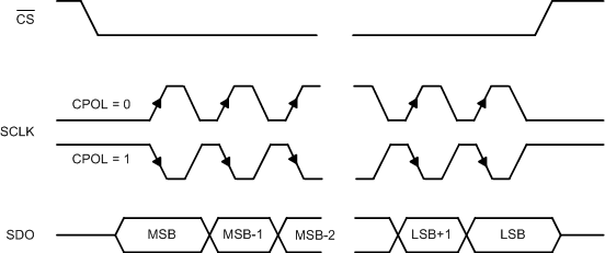
TLA2518 1-sdo_cpha0.gif
Figure 26. Standard SPI Timing Protocol
(CPHA = 0)
TLA2518 1-sdo_cpha1.gif
Figure 27. Standard SPI Timing Protocol
(CPHA = 1)