JAJSHO0J August 1983 – November 2023 TLC555
PRODUCTION DATA
- 1
- 1 特長
- 2 アプリケーション
- 3 概要
- 4 Pin Configuration and Functions
-
5 Specifications
- 5.1 Absolute Maximum Ratings
- 5.2 ESD Ratings
- 5.3 Recommended Operating Conditions
- 5.4 Thermal Information
- 5.5 Electrical Characteristics: VDD = 2 V for TLC555C, VDD = 3 V for TLC555I
- 5.6 Electrical Characteristics: VDD = 5 V
- 5.7 Electrical Characteristics: VDD = 15 V
- 5.8 Timing Characteristics
- 5.9 Typical Characteristics
- 6 Detailed Description
- 7 Application and Implementation
- 8 Device and Documentation Support
- 9 Revision History
- 10Mechanical, Packaging, and Orderable Information
パッケージ・オプション
メカニカル・データ(パッケージ|ピン)
サーマルパッド・メカニカル・データ
- PS|8
発注情報
4 Pin Configuration and Functions
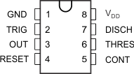
 Figure 4-1 D, P, PS, and JG Packages, 8-Pin SOIC, PDIP,
SOP, and CDIP (Top View)
Figure 4-1 D, P, PS, and JG Packages, 8-Pin SOIC, PDIP,
SOP, and CDIP (Top View)Table 4-1 Pin Functions: D, P, PS, and JG
Packages
| PIN | TYPE | DESCRIPTION | |
|---|---|---|---|
| NAME | NO. | ||
| CONT | 5 | Input | Controls comparator thresholds. Outputs 2/3 VDD and allows bypass capacitor connection. |
| DISCH | 7 | Output | Open collector output to discharge timing capacitor. |
| GND | 1 | — | Ground. |
| NC | — | — | No internal connection. |
| OUT | 3 | Output | High current timer output signal. |
| RESET | 4 | Input | Active low reset input forces output and discharge low. |
| THRES | 6 | Input | End of timing input. THRES > CONT sets output low and discharge low. |
| TRIG | 2 | Input | Start of timing input. TRIG < 1/2 CONT sets output high and discharge open. |
| VDD | 8 | — | Power-supply voltage. |
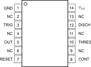
 Figure 4-2 PW Package, 14-Pin TSSOP
(Top View)
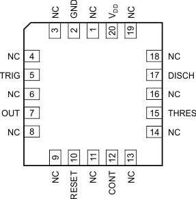
 Figure 4-3 FK Package, 20-Pin LCCC
(Top View)
Figure 4-3 FK Package, 20-Pin LCCC
(Top View)Table 4-2 Pin Functions: PW and FK
| PIN | TYPE | DESCRIPTION | ||
|---|---|---|---|---|
| NAME | NO. | |||
| PW (TSSOP) | FK (LCCC) | |||
| CONT | 8 | 12 | Input | Controls comparator thresholds. Outputs 2/3 VDD and allows bypass capacitor connection. |
| DISCH | 12 | 17 | Output | Open-collector output to discharge timing capacitor. |
| GND | 1 | 2 | — | Ground. |
| NC | 2, 4, 6, 9, 11, 13 |
1, 3, 4, 6, 8, 9, 11, 13, 14, 16, 18, 19 |
— | No internal connection. |
| OUT | 5 | 7 | Output | High current timer output signal. |
| RESET | 7 | 10 | Input | Active low reset input forces output and discharge low. |
| THRES | 10 | 15 | Input | End of timing input. THRES > CONT sets output low and discharge low. |
| TRIG | 3 | 5 | Input | Start of timing input. TRIG < 1/2 CONT sets output high and discharge open. |
| VDD | 14 | 20 | — | Power-supply voltage. |