SCLS715A March 2009 – November 2015 TLC59208F
PRODUCTION DATA.
- 1 Features
- 2 Applications
- 3 Description
- 4 Revision History
- 5 Description (continued)
- 6 Pin Configuration and Functions
- 7 Specifications
- 8 Parameter Measurement Information
-
9 Detailed Description
- 9.1 Overview
- 9.2 Functional Block Diagram
- 9.3 Feature Description
- 9.4 Device Functional Modes
- 9.5 Programming
- 9.6
Register Maps
- 9.6.1
Register Descriptions
- 9.6.1.1 Mode Register 1 (MODE1)
- 9.6.1.2 Mode Register 2 (MODE2)
- 9.6.1.3 Individual Brightness Control Registers (PWM0-PWM7)
- 9.6.1.4 Group Duty Cycle Control Register (GRPPWM)
- 9.6.1.5 Group Frequency Register (GRPFREQ)
- 9.6.1.6 LED Driver Output State Registers (LEDOUT0, LEDOUT1)
- 9.6.1.7 I2C Bus Sub-Address Registers 1 to 3 (SUBADR1-SUBADR3)
- 9.6.1.8 LED All Call I2C Bus Address Register (ALLCALLADR)
- 9.6.1
Register Descriptions
- 10Application and Implementation
- 11Power Supply Recommendations
- 12Layout
- 13Device and Documentation Support
- 14Mechanical, Packaging, and Orderable Information
パッケージ・オプション
メカニカル・データ(パッケージ|ピン)
サーマルパッド・メカニカル・データ
- RGY|16
発注情報
10 Application and Implementation
NOTE
Information in the following applications sections is not part of the TI component specification, and TI does not warrant its accuracy or completeness. TI’s customers are responsible for determining suitability of components for their purposes. Customers should validate and test their design implementation to confirm system functionality.
10.1 Application Information
10.1.1 Setting LED Current
The LED current is primarily dependent on the supply voltage, the forward voltage of the LED, and the series resistor (RSET). In many applications the supply voltage and LED forward voltage cannot be adjusted. Hence, RSET is utilized to adjust the LED current. This calculation is discussed in detail in the typical application example.
10.1.2 PWM Brightness Dimming
The perceived brightness of the LEDs can be adjusted by use of PWM dimming. For example, an LED driven at 50% duty cycle will appear less bright than it would at 100% duty cycle. The TLC59208F offers duty cycle control for each individual channel and also offers group duty cycle control. Refer to the Register Map for details regarding programmable duty cycle.
10.2 Typical Application
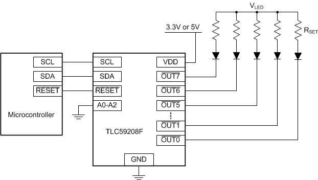
This application example provides guidance on how to set the LED current using the TLC59208F.
 Figure 20. Typical Application
10.2.1 Design Requirements
For this design example, use Table 12 the following as the input parameters.
Table 12. Design Parameters
| DESIGN PARAMETER | EXAMPLE VALUE | |
|---|---|---|
| VLED | Supply voltage that powers the LED | 5-V |
| VF | Forward voltage across the LED | 3-V |
| ILED | Current flowing through the LED | 6-mA |
| RON | Resistance across open-drain output | 1.5-Ω |
10.2.2 Detailed Design Procedure
In the LED current path, there are three voltage drops that must be considered:
- Drop across the series resistor (VRSET)
- Drop across the LED (VF)
- Drop across the open-drain output channel (VO)
The drop across the LED is defined above as VF = 3 V. The drop across the open-drain output is calculated as RON × ILED (1.5 × 0.006 = 0.009 V). The remaining voltage must be across the series resistor:
After calculating VRSET, we can calculate RSET:
10.2.3 Application Curve
The following graph shows the typical LED Current as a function of RSET and VF. The graph assumes that VLED = 5 V.
 Figure 21. LED Current vs RSET