SCLS715A March 2009 – November 2015 TLC59208F
PRODUCTION DATA.
- 1 Features
- 2 Applications
- 3 Description
- 4 Revision History
- 5 Description (continued)
- 6 Pin Configuration and Functions
- 7 Specifications
- 8 Parameter Measurement Information
-
9 Detailed Description
- 9.1 Overview
- 9.2 Functional Block Diagram
- 9.3 Feature Description
- 9.4 Device Functional Modes
- 9.5 Programming
- 9.6
Register Maps
- 9.6.1
Register Descriptions
- 9.6.1.1 Mode Register 1 (MODE1)
- 9.6.1.2 Mode Register 2 (MODE2)
- 9.6.1.3 Individual Brightness Control Registers (PWM0-PWM7)
- 9.6.1.4 Group Duty Cycle Control Register (GRPPWM)
- 9.6.1.5 Group Frequency Register (GRPFREQ)
- 9.6.1.6 LED Driver Output State Registers (LEDOUT0, LEDOUT1)
- 9.6.1.7 I2C Bus Sub-Address Registers 1 to 3 (SUBADR1-SUBADR3)
- 9.6.1.8 LED All Call I2C Bus Address Register (ALLCALLADR)
- 9.6.1
Register Descriptions
- 10Application and Implementation
- 11Power Supply Recommendations
- 12Layout
- 13Device and Documentation Support
- 14Mechanical, Packaging, and Orderable Information
パッケージ・オプション
メカニカル・データ(パッケージ|ピン)
サーマルパッド・メカニカル・データ
- RGY|16
発注情報
7 Specifications
7.1 Absolute Maximum Ratings
over operating free-air temperature range (unless otherwise noted)(1)| MIN | MAX | UNIT | |||
|---|---|---|---|---|---|
| VCC | Supply voltage | 0 | 7 | V | |
| VI | Input voltage | –0.4 | 7 | V | |
| VO | Output voltage | –0.5 | 20 | V | |
| IO | Continuous output current | 50 | mA | ||
| θJA | Package thermal impedance | PW package(2) | 108 | °C/W | |
| RGY package(3) | 39 | ||||
| PD | Power Dissipation, TA = 25 °C, JESD 51-7 | PW package | 0.90 | W | |
| RGY package | 2.08 | ||||
| TJ | Junction temperature | –40 | 150 | °C | |
| Tstg | Storage temperature | –55 | 150 | °C | |
(1) Stresses beyond those listed under Absolute Maximum Ratings may cause permanent damage to the device. These are stress ratings only, which do not imply functional operation of the device at these or any other conditions beyond those indicated under Recommended Operating Conditions. Exposure to absolute-maximum-rated conditions for extended periods may affect device reliability.
(2) The package thermal impedance is calculated in accordance with JESD 51-7.
(3) The package thermal impedance is calculated in accordance with JESD 51-5.
7.2 ESD Ratings
| VALUE | UNIT | |||
|---|---|---|---|---|
| V(ESD) | Electrostatic discharge | Human body model (HBM), per ANSI/ESDA/JEDEC JS-001(1) | ±2000 | V |
| Charged-device model (CDM), per JEDEC specification JESD22-C101(2) | ±500 | |||
(1) JEDEC document JEP155 states that 500-V HBM allows safe manufacturing with a standard ESD control process.
(2) JEDEC document JEP157 states that 250-V CDM allows safe manufacturing with a standard ESD control process.
7.3 Recommended Operating Conditions
over operating free-air temperature range (unless otherwise noted)(1)| MIN | MAX | UNIT | ||||
|---|---|---|---|---|---|---|
| VCC | Supply voltage | 3 | 5.5 | V | ||
| VIH | High-level input voltage | SCL, SDA, RESET, A0, A1, A2 | 0.7 × VCC | 5.5 | V | |
| VIL | Low-level input voltage | SCL, SDA, RESET, A0, A1, A2 | 0 | 0.3 × VCC | V | |
| VO | Output voltage | OUT0 to OUT7 | 17 | V | ||
| IOL | Low-level output current | SDA | VCC = 3 V | 20 | mA | |
| VCC = 4.5 V | 30 | |||||
| IO | Output current | OUT0 to OUT7 | 50 | mA | ||
| TA | Operating free-air temperature | –40 | 85 | °C | ||
(1) All unused inputs of the device must be held at VCC or GND to ensure proper device operation.
7.4 Thermal Information
| THERMAL METRIC(1) | TLC59208F | UNIT | ||
|---|---|---|---|---|
| PW (TSSOP) | RGY (VQFN) | |||
| 16 PINS | 16 PINS | |||
| RθJA | Junction-to-ambient thermal resistance | 108 | 39 | °C/W |
(1) For more information about traditional and new thermal metrics, see the Semiconductor and IC Package Thermal Metrics application report, SPRA953.
7.5 Electrical Characteristics
VCC = 3 V to 5.5 V, TA = –40°C to 85°C (unless otherwise noted)| PARAMETER | TEST CONDITIONS | MIN | TYP(1) | MAX | UNIT | ||||
|---|---|---|---|---|---|---|---|---|---|
| II | Input/output leakage current | SCL, SDA, A0, A1, A2, RESET | VI = VCC or GND | ±0.3 | μA | ||||
| Output leakage current | OUT0 to OUT7 | VO = 17 V, TJ = 25°C | 0.5 | μA | |||||
| VPOR | Power-on reset voltage | 2.5 | V | ||||||
| IOL | Low-level output current | SDA | VCC = 3 V, VOL = 0.4 V | 20 | mA | ||||
| VCC = 4.5 V, VOL = 0.4 V | 30 | ||||||||
| VOL | Low-level output voltage | OUT0 to OUT7 | VCC = 3 V, IOL = 50 mA | 108 | 185 | mV | |||
| VCC = 4.5 V, IOL = 50 mA | 90 | 165 | |||||||
| rON | ON-state resistance | OUT0 to OUT7 | VCC = 3 V, IOL = 50 mA | 2 | 3.75 | Ω | |||
| VCC = 4.5 V, IOL = 50 mA | 1.8 | 3.3 | |||||||
| TSD | Thermal shutdown temperature(2) | 150 | 175 | 200 | °C | ||||
| THYS | Restart hysteresis | 15 | °C | ||||||
| Ci | Input capacitance | SCL, A0, A1, A2, RESET | VI = VCC or GND | 6 | pF | ||||
| Cio | Input/output capacitance | SDA | VI = VCC or GND | 8 | pF | ||||
| ICC | Supply current | VCC = 3.3 V, OUT0 to OUT7 = OFF | 5 | mA | |||||
| VCC = 5.5 V, OUT0 to OUT7 = OFF | 8 | ||||||||
(1) All typical values are at TJ = 25°C.
(2) Specified by design, not production tested.
7.6 I2C Interface Timing Requirements
TA = –40°C to 85°C| STANDARD-MODE I2C BUS |
FAST-MODE I2C BUS |
FAST-MODE PLUS I2C BUS |
UNIT | |||||
|---|---|---|---|---|---|---|---|---|
| MIN | MAX | MIN | MAX | MIN | MAX | |||
| I2C INTERFACE | ||||||||
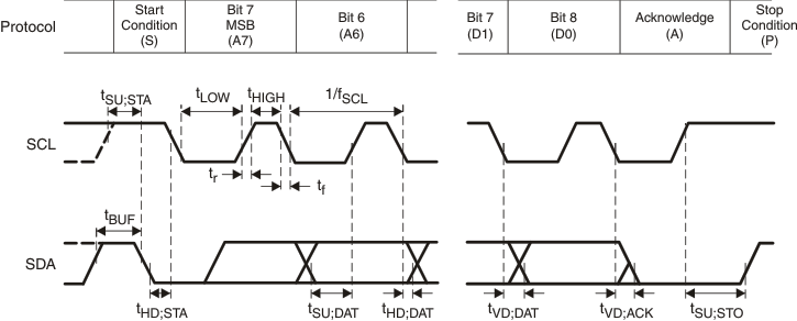
| fSCL | SCL clock frequency | 0 | 100 | 0 | 400 | 0 | 1000 | kHz |
| tBUF | I2C bus free time between stop and start | 4.7 | 1.3 | 0.5 | μs | |||
| tHD;STA | Hold time (repeated) Start condition | 4 | 0.6 | 0.26 | μs | |||
| tSU;STA | Set-up time for a repeated Start condition | 4.7 | 0.6 | 0.26 | μs | |||
| tSU;STO | Set-up time for Stop condition | 4 | 0.6 | 0.26 | μs | |||
| tHD;DAT | Data hold time | 0 | 0 | 0 | ns | |||
| tVD;ACK | Data valid acknowledge time(1) | 0.3 | 3.45 | 0.1 | 0.9 | 0.05 | 0.45 | μs |
| tVD;DAT | Data valid time(2) | 0.3 | 3.45 | 0.1 | 0.9 | 0.05 | 0.45 | μs |
| tSU;DAT | Data set-up time | 250 | 100 | 50 | ns | |||
| tLOW | Low period of the SCL clock | 4.7 | 1.3 | 0.5 | μs | |||
| tHIGH | High period of the SCL clock | 4 | 0.6 | 0.26 | μs | |||
| tf | Fall time of both SDA and SCL signals(4) (5) | 300 | 20+0.1Cb (3) | 300 | 120 | ns | ||
| tr | Rise time of both SDA and SCL signals | 1000 | 20+0.1Cb (3) | 300 | 120 | ns | ||
| tSP | Pulse width of spikes that must be suppressed by the input filter(6) | 50 | 50 | 50 | ns | |||
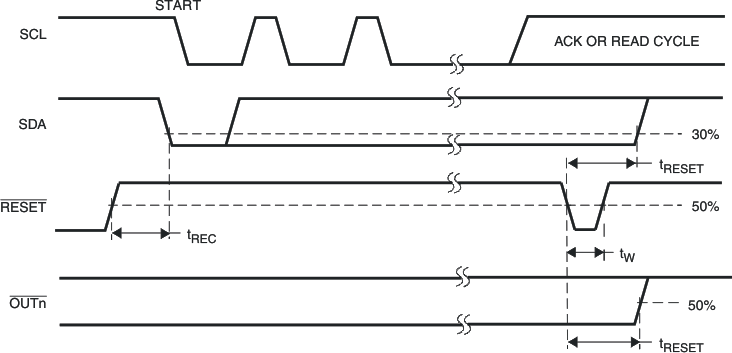
| RESET | ||||||||
| tW | Reset pulse width | 10 | 10 | 10 | ns | |||
| tREC | Reset recovery time | 0 | 0 | 0 | ns | |||
| tRESET | Time to reset(7) (8) | 400 | 400 | 400 | ns | |||
(1) tVD;ACK = time for Acknowledgement signal from SCL low to SDA (out) low.
(2) tVD;DAT = minimum time for SDA data out to be valid following SCL low.
(3) Cb = total capacitance of one bus line in pF.
(4) A master device must internally provide a hold time of at least 300 ns for the SDA signal (refer to the VIL of the SCL signal) in order to bridge the undefined region of SCLs falling edge.
(5) The maximum tf for the SDA and SCL bus lines is specified at 300 ns. The maximum fall time (tf) for the SDA output stage is specified at 250 ns. This allows series protection resistors to be connected between the SDA and the SCL pins and the SDA/SCL bus lines without exceeding the maximum specified tf.
(6) Input filters on the SDA and SCL inputs suppress noise spikes less than 50 ns
(7) Resetting the device while actively communicating on the bus may cause glitches or errant Stop conditions.
(8) Upon reset, the full delay will be the sum of tRESET and the RC time constant of the SDA bus.
 Figure 1. Definition of RESET Timing
 Figure 2. Definition of Timing

NOTE:
Rise and fall times refer to VIL and VIH.7.7 Typical Characteristics

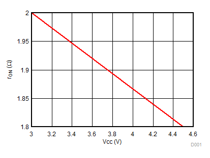
IOL = 50 mA
Figure 4. rON vs Vcc

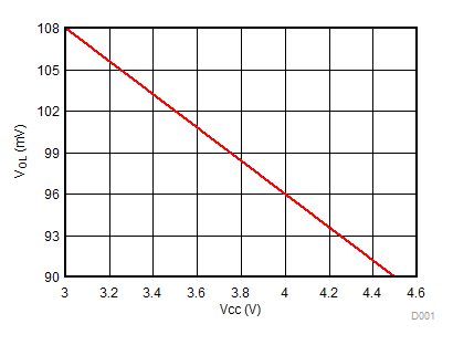
IOL = 50 mA
Figure 5. VOL vs Vcc