-
TLC5940 16-Channel LED Driver With DOT Correction and Grayscale PWM Control
- 1 Features
- 2 Applications
- 3 Description
- 4 Revision History
- 5 Pin Configuration and Functions
- 6 Specifications
- 7 Parameter Measurement Information
- 8 Detailed Description
- 9 Application and Implementation
- 10Power Supply Recommendations
- 11Layout
- 12Device and Documentation Support
- 13Mechanical, Packaging, and Orderable Information
- IMPORTANT NOTICE
パッケージ・オプション
メカニカル・データ(パッケージ|ピン)
サーマルパッド・メカニカル・データ
発注情報
TLC5940 16-Channel LED Driver With DOT Correction and Grayscale PWM Control
1 Features
- 16 Channels
- 12 bit (4096 Steps) Grayscale PWM Control
- Dot Correction
- 6 bit (64 Steps)
- Storable in Integrated EEPROM
- Drive Capability (Constant-Current Sink)
- 0 mA to 60 mA (VCC < 3.6 V)
- 0 mA to 120 mA (VCC > 3.6 V)
- LED Power Supply Voltage up to 17 V
- VCC = 3 V to 5.5 V
- Serial Data Interface
- Controlled In-Rush Current
- 30 MHz Data Transfer Rate
- CMOS Level I/O
- Error Information
- LOD: LED Open Detection
- TEF: Thermal Error Flag
2 Applications
- Monocolor, Multicolor, Full-Color LED Displays
- LED Signboards
- Display Backlighting
- General, High-Current LED Drive
3 Description
The TLC5940 is a 16-channel, constant-current sink LED driver. Each channel has an individually adjustable 4096-step grayscale PWM brightness control and a 64-step, constant-current sink (dot correction). The dot correction adjusts the brightness variations between LED channels and other LED drivers. The dot correction data is stored in an integrated EEPROM. Both grayscale control and dot correction are accessible through a serial interface. A single external resistor sets the maximum current value of all 16 channels.
The TLC5940 features two error information circuits. The LED open detection (LOD) indicates a broken or disconnected LED at an output terminal. The thermal error flag (TEF) indicates an overtemperature condition.
Device Information(1)
| PART NUMBER | PACKAGE | BODY SIZE (NOM) |
|---|---|---|
| TLC5940 | PDIP (28) | 35.69 mm × 6.73 mm |
| HTSSOP (28) | 9.70 mm × 4.40 mm | |
| VQFN (32) | 5.00 mm × 5.00 mm |
- For all available packages, see the orderable addendum at the end of the datasheet.
Block Diagram

4 Revision History
Changes from C Revision (October 2007) to D Revision
- Added ESD Ratings table, Feature Description section, Device Functional Modes, Application and Implementation section, Power Supply Recommendations section, Layout section, Device and Documentation Support section, and Mechanical, Packaging, and Orderable Information section.Go
Changes from B Revision (September 2007) to C Revision
- Changed tsu5 setup time from: 30 ms to: 30 nsGo
5 Pin Configuration and Functions


Pin Functions
| PIN | TYPE | DESCRIPTION | |||
|---|---|---|---|---|---|
| NAME | DIP NO. | PWP NO. | RHB NO. | ||
| BLANK | 23 | 2 | 31 | I | Blank all outputs. When BLANK = H, all OUTn outputs are forced OFF. GS counter is also reset. When BLANK = L, OUTn are controlled by grayscale PWM control. |
| DCPRG | 19 | 26 | 25 | I | Switch DC data input. When DCPRG = L, DC is connected to EEPROM. When DCPRG = H, DC is connected to the DC register. DCPRG also controls EEPROM writing, when VPRG = V(PRG). EEPROM data = 3 Fh (default) |
| GND | 22 | 1 | 30 | G | Ground |
| GSCLK | 18 | 25 | 24 | I | Reference clock for grayscale PWM control |
| IREF | 20 | 27 | 26 | I | Reference current terminal |
| NC | — | — | 12 | — | No connection |
| — | — | 13 | |||
| — | — | 28 | |||
| — | — | 29 | |||
| OUT0 | 28 | 7 | 4 | O | Constant current output |
| OUT1 | 1 | 8 | 5 | O | Constant current output |
| OUT2 | 2 | 9 | 6 | O | Constant current output |
| OUT3 | 3 | 10 | 7 | O | Constant current output |
| OUT4 | 4 | 11 | 8 | O | Constant current output |
| OUT5 | 5 | 12 | 9 | O | Constant current output |
| OUT6 | 6 | 13 | 10 | O | Constant current output |
| OUT7 | 7 | 14 | 11 | O | Constant current output |
| OUT8 | 8 | 15 | 14 | O | Constant current output |
| OUT9 | 9 | 16 | 15 | O | Constant current output |
| OUT10 | 10 | 17 | 16 | O | Constant current output |
| OUT11 | 11 | 18 | 17 | O | Constant current output |
| OUT12 | 12 | 19 | 18 | O | Constant current output |
| OUT13 | 13 | 20 | 19 | O | Constant current output |
| OUT14 | 14 | 21 | 20 | O | Constant current output |
| OUT15 | 15 | 22 | 21 | O | Constant current output |
| SCLK | 25 | 4 | 1 | I | Serial data shift clock |
| SIN | 26 | 5 | 2 | I | Serial data input |
| SOUT | 17 | 24 | 23 | O | Serial data output |
| VCC | 21 | 28 | 27 | I | Power supply voltage |
| VPRG | 27 | 6 | 3 | I | Multifunction input pin. When VPRG = GND, the device is in GS mode. When VPRG = VCC, the device is in DC mode. When VPRG = V(VPRG), DC register data can programmed into DC EEPROM with DCPRG=HIGH. EEPROM data = 3 Fh (default) |
| XERR | 16 | 23 | 22 | O | Error output. XERR is an open-drain terminal. XERR goes L when LOD or TEF is detected. |
| XLAT | 24 | 3 | 32 | I | Level triggered latch signal. When XLAT = high, the TLC5940 writes data from the input shift register to either GS register (VPRG = low) or DC register (VPRG = high). When XLAT = low, the data in GS or DC register is held constant. |
6 Specifications
6.1 Absolute Maximum Ratings
over operating free-air temperature range (unless otherwise noted)(1)| MIN | MAX | UNIT | ||
|---|---|---|---|---|
| Input voltage(2) | VCC | –0.3 | 6 | V |
| V(BLANK), V(DCPRG), V(SCLK), V(XLAT), V(SIN), V(GSCLK), V(IREF) | –0.3 | VCC +0.3 | V | |
| Output voltage | V(SOUT), V(XERR) | –0.3 | VCC +0.3 | V |
| V(OUT0) to V(OUT15) | –0.3 | 18 | V | |
| Output current (dc) | 130 | mA | ||
| EEPROM program range | V(VPRG) | –0.3 | 24 | V |
| EEPROM write cycles | 50 | — | ||
| Storage temperature, Tstg | –55 | 150 | °C | |
6.2 ESD Ratings
| VALUE | UNIT | |||
|---|---|---|---|---|
| V(ESD) | Electrostatic discharge | Human-body model (HBM), per ANSI/ESDA/JEDEC JS-001(1) | ±2000 | V |
| Charged-device model (CDM), per JEDEC specification JESD22-C101(2) | ±500 | |||
6.3 Recommended Operating Conditions
| MIN | NOM | MAX | UNIT | |||
|---|---|---|---|---|---|---|
| DC CHARACTERISTICS | ||||||
| VCC | Supply Voltage | 3 | 5.5 | V | ||
| V O | Voltage applied to output (OUT0–OUT15) | 17 | V | |||
| VIH | High-level input voltage | 0.8 VCC | VCC | V | ||
| VIL | Low-level input voltage | GND | 0.2 VCC | V | ||
| IOH | High-level output current | VCC = 5 V at SOUT | –1 | mA | ||
| IOL | Low-level output current | VCC = 5 V at SOUT, XERR | 1 | mA | ||
| IOLC | Constant output current | OUT0 to OUT15, VCC < 3.6 V | 60 | mA | ||
| OUT0 to OUT15, VCC > 3.6 V | 120 | mA | ||||
| V(VPRG) | EEPROM program voltage | 20 | 22 | 23 | V | |
| TA | Operating free-air temperature range | -40 | 85 | °C | ||
| AC CHARACTERISTICS
VCC = 3 V to 5.5 V, TA = –40°C to 85°C (unless otherwise noted) |
||||||
| f(SCLK) | Data shift clock frequency | SCLK | 30 | MHz | ||
| f(GSCLK) | Grayscale clock frequency | GSCLK | 30 | MHz | ||
| twh0/twl0 | SCLK pulse duration | SCLK = H/L (see Figure 11) | 16 | ns | ||
| twh1/twl1 | GSCLK pulse duration | GSCLK = H/L (see Figure 11) | 16 | ns | ||
| twh2 | XLAT pulse duration | XLAT = H (see Figure 11) | 20 | ns | ||
| twh3 | BLANK pulse duration | BLANK = H (see Figure 11) | 20 | ns | ||
| tsu0 | Setup time | SIN to SCLK ↑(1) (see Figure 11) | 5 | ns | ||
| tsu1 | SCLK ↓ to XLAT ↑ (see Figure 11) | 10 | ns | |||
| tsu2 | VPRG ↑ ↓ to SCLK ↑ (see Figure 11) | 10 | ns | |||
| tsu3 | VPRG ↑ ↓XLAT ↑ (see Figure 11) | 10 | ns | |||
| tsu4 | BLANK ↓ to GSCLK ↑ (see Figure 11) | 10 | ns | |||
| tsu5 | XLAT ↑ to GSCLK ↑ (see Figure 11) | 30 | ns | |||
| tsu6 | VPRG ↑ to DCPRG ↑ (see Figure 16) | 1 | ms | |||
| th0 | Hold Time | SCLK ↑ to SIN (see Figure 11) | 3 | ns | ||
| th1 | XLAT ↓ to SCLK ↑ (see Figure 11) | 10 | ns | |||
| th2 | SCLK ↑ to VPRG ↑ ↓ (see Figure 11) | 10 | ns | |||
| th3 | XLAT ↓ to VPRG ↑ ↓ (see Figure 11) | 10 | ns | |||
| th4 | GSCLK ↑ to BLANK ↑ (see Figure 11) | 10 | ns | |||
| th5 | DCPRG ↓ to VPRG ↓ (see Figure 11) | 1 | ms | |||
| tprog | Programming time for EEPROM (see Figure 16) | 20 | ms | |||
6.4 Thermal Information
| THERMAL METRIC(1) | TLC5940 | UNIT | ||
|---|---|---|---|---|
| PWP (HTSSOP) | RHB (VQFN) | |||
| 28 PINS | 32 PINS | |||
| RθJA | Junction-to-ambient thermal resistance | 36.7 | 34.3 | °C/W |
| RθJC(top) | Junction-to-case (top) thermal resistance | 18.9 | 36.8 | °C/W |
| RθJB | Junction-to-board thermal resistance | 15.9 | 8.5 | °C/W |
| ψJT | Junction-to-top characterization parameter | 0.6 | 0.3 | °C/W |
| ψJB | Junction-to-board characterization parameter | 15.8 | 8.7 | °C/W |
| RθJC(bot) | Junction-to-case (bottom) thermal resistance | 2.3 | 1.6 | °C/W |
6.5 Electrical Characteristics
VCC = 3 V to 5.5 V, TA = –40°C to 85°C (unless otherwise noted)| PARAMETER | TEST CONDITIONS | MIN | TYP | MAX | UNIT | |
|---|---|---|---|---|---|---|
| VOH | High-level output voltage | IOH = -1 mA, SOUT | VCC –0.5 | V | ||
| VOL | Low-level output voltage | IOL = 1 mA, SOUT | 0.5 | V | ||
| II | Input current | VI = VCC or GND; BLANK, DCPRG, GSCLK, SCLK, SIN, XLAT | –1 | 1 | μA | |
| VI = GND; VPRG | –1 | 1 | ||||
| VI = VCC; VPRG | 50 | |||||
| VI = 22 V; VPRG; DCPRG = VCC | 4 | 10 | mA | |||
| ICC | Supply current | No data transfer, all output OFF, VO = 1 V, R(IREF) = 10 kΩ |
0.9 | 6 | mA | |
| No data transfer, all output OFF, VO = 1 V, R(IREF) = 1.3 kΩ |
5.2 | 12 | ||||
| Data transfer 30MHz, all output ON, VO = 1 V, R(IREF) = 1.3 kΩ |
16 | 25 | ||||
| Data transfer 30MHz, all output ON, VO = 1 V, R(IREF) = 640 Ω |
30 | 60 | ||||
| IO(LC) | Constant sink current (see Figure 10) | All output ON, VO = 1 V, R(IREF) = 640 Ω | 54 | 61 | 69 | mA |
| Ilkg | Leakage output current | All output OFF, VO = 15 V, R(IREF) = 640 Ω, OUT0 to OUT15 |
0.1 | μA | ||
| ΔIO(LC0) | Constant sink current error (see Figure 10) | All output ON, VO = 1 V, R(IREF) = 640 Ω, OUT0 to OUT15, –20°C to 85°C |
±1% | ±4% | ||
| All output ON, VO = 1V, R(IREF) = 640 Ω, OUT0 to OUT15(1) |
±1% | ±8% | ||||
| All output ON, VO = 1V, R(IREF) = 320 Ω, OUT0 to OUT15, –20°C to 85°C |
±1% | ±6% | ||||
| All output ON, VO = 1V, R(IREF) = 320 Ω, VCC = 4.5 V to 5.5 V, OUT0 to OUT15(1) |
±1% | ±8% | ||||
| ΔIO(LC1) | Constant sink current error (see Figure 10) | Device to device, Averaged current from OUT0 to OUT15, R(IREF) = 1920 Ω (20 mA)(2) | –2% +0.4% |
±4% | ||
| ΔIO(LC2) | Constant sink current error (see Figure 10) | Device to device, Averaged current from OUT0 to OUT15, R(IREF) = 480 Ω (80 mA)(2) | –2.7% +2% |
±4% | ||
| ΔIO(LC3) | Line regulation (see Figure 10) | All output ON, VO = 1V, R(IREF) = 640 Ω OUT0 to OUT15, VCC = 3 V to 5.5 V(3) |
±1 | ±4 | %/V | |
| All output ON, VO = 1V, R(IREF) = 320 Ω , OUT0 to OUT15, VCC = 3 V to 5.5 V(3) |
±1 | ±6 | %/V | |||
| ΔIO(LC4) | Load regulation (see Figure 10) | All output ON, VO = 1 V to 3 V, R(IREF) = 640 Ω, OUT0 to OUT15(4) |
±2 | ±6 | %/V | |
| All output ON, VO = 1 V to 3 V, R(IREF) = 320 Ω, OUT0 to OUT15(4) |
±2 | ±8 | %/V | |||
| T(TEF) | Thermal error flag threshold | Junction temperature(5) | 150 | 170 | °C | |
| V(LED) | LED open detection threshold | 0.3 | 0.4 | V | ||
| V(IREF) | Reference voltage output |
R(IREF) = 640 Ω | 1.20 | 1.24 | 1.28 | V |
6.6 Switching Characteristics
VCC = 3V to 5.5V, TA = -40°C to 85°C (unless otherwise noted)| PARAMETER | TEST CONDITIONS | MIN | TYP | MAX | UNIT | |
|---|---|---|---|---|---|---|
| tr0 | Rise time | SOUT | 16 | ns | ||
| tr1 | OUTn, VCC = 5 V, TA = 60°C, DCn = 3 Fh | 10 | 30 | |||
| tf0 | Fall time | SOUT | 16 | ns | ||
| tf1 | OUTn, VCC = 5 V, TA = 60°C, DCn = 3 Fh | 10 | 30 | |||
| tpd0 | Propagation delay time | SCLK to SOUT (see Figure 11) | 30 | ns | ||
| tpd1 | BLANK to OUT0 | 60 | ns | |||
| tpd2 | OUTn to XERR (see Figure 11) | 1000 | ns | |||
| tpd3 | GSCLK to OUT0 (see Figure 11) | 60 | ns | |||
| tpd4 | XLAT to IOUT (dot correction) (see Figure 11) | 60 | ns | |||
| tpd5 | DCPRG to OUT0 (see Figure 11) | 30 | ns | |||
| td | Output delay time | OUTn to OUT(n+1) (see Figure 11) | 20 | 30 | ns | |
| ton-err | Output on-time error | touton– Tgsclk (see Figure 11), GSn = 01h, GSCLK = 11 MHz | 10 | –50 | –90 | ns |
6.7 Typical Characteristics
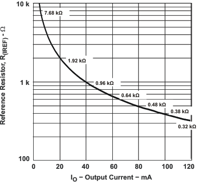 Figure 1. Reference Resistor vs Output Current
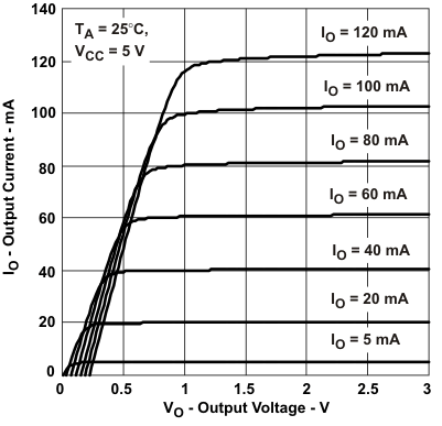 Figure 3. Output Current vs Output Voltage
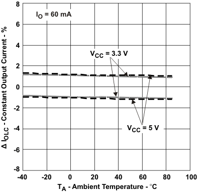 Figure 5. Constant Output Current, ΔIOLC
vs Ambient Temperature
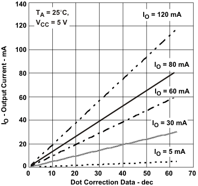 Figure 7. Output Current
 vs DOT Correction Linearity (ABS Value)
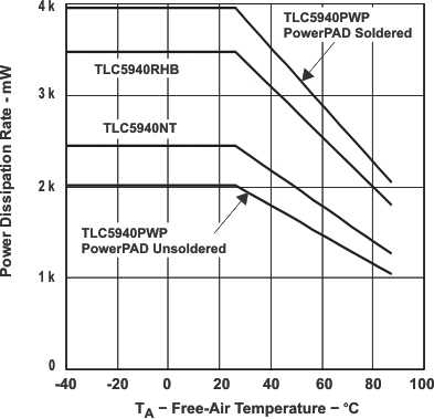 Figure 2. Power Dissipation Rate vs Free-Air Temperature
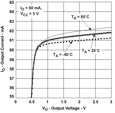 Figure 4. Output Current vs Output Voltage
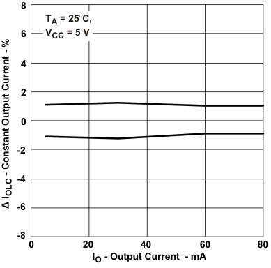 Figure 6. Constant Output Current, ΔIOLC
vs Output Current
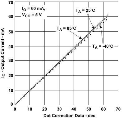 Figure 8. Output Current
 vs DOT Correction Linearity (ABS Value)
7 Parameter Measurement Information
Resistor values are equivalent resistances, and they are not tested.
 Figure 9. Input and Output Equivalent Circuits
 Figure 10. Parameter Measurement Circuits
7.1 Test Parameter Equations


