SLDS165A December 2008 – December 2014 TLC5941-Q1
PRODUCTION DATA.
- 1 Features
- 2 Applications
- 3 Description
- 4 Revision History
- 5 Pin Configuration and Functions
- 6 Specifications
- 7 Parameter Measurement Information
- 8 Detailed Description
- 9 Application and Implementation
- 10Power Supply Recommendations
- 11Layout
- 12Device and Documentation Support
- 13Mechanical, Packaging, and Orderable Information
11 Layout
11.1 Layout Guidelines
In order to prevent thermal shutdown, TJ must be less than 150ºC. If the input voltage is very high, the power dissipation might be large. Currently there is the HTSSOP package which has good thermal impedance, but at the same time, the PCB layout is also very important. Good PCB design can optimize heat transfer, which is absolutely essential for the long-term reliability of the device.
- Maximize the copper coverage on the PCB to increase the thermal conductivity of the board, because the major heat-flow path from the package to the ambient is through the copper on the PCB. Maximum copper is extremely important when there are not any heat sinks attached to the PCB on the other side of the package.
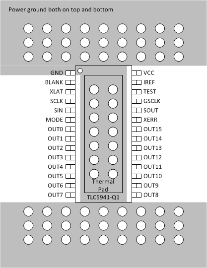
- Add as many thermal vias as possible directly under the package ground pad to optimize the thermal conductivity of the board.
- All thermal vias should be either plated shut or plugged and capped on both sides of the board to prevent solder voids. To ensure reliability and performance, the solder coverage should be at least 85 percent.
11.2 Layout Example
 Figure 25. PCB Layout Example