SLDS165A December 2008 – December 2014 TLC5941-Q1
PRODUCTION DATA.
- 1 Features
- 2 Applications
- 3 Description
- 4 Revision History
- 5 Pin Configuration and Functions
- 6 Specifications
- 7 Parameter Measurement Information
- 8 Detailed Description
- 9 Application and Implementation
- 10Power Supply Recommendations
- 11Layout
- 12Device and Documentation Support
- 13Mechanical, Packaging, and Orderable Information
5 Pin Configuration and Functions
PWP Package
28-Pin HSSOP With Thermal Pad
Top View
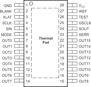
Pin Functions
| PIN | I/O | DESCRIPTION | |
|---|---|---|---|
| NAME | NO. | ||
| BLANK | 2 | I | Blank all outputs. When BLANK = H, all OUTn outputs are forced OFF. GS counter is also reset. When BLANK = L, OUTn are controlled by grayscale PWM control. This pin should be pull up to high before micro-controller or digital signal processor sending control signal to device. A pull-up resistor to VCC is needed. |
| GND | 1 | G | Ground |
| GSCLK | 25 | I | Reference clock for grayscale PWM control |
| IREF | 27 | I/O | Reference current terminal |
| MODE | 6 | I | Input mode-change pin. When MODE = GND, the device is in GS mode. When MODE = VCC, the device is in DC mode. |
| OUT0 | 7 | O | Constant-current output |
| OUT1 | 8 | O | Constant-current output |
| OUT2 | 9 | O | Constant-current output |
| OUT3 | 10 | O | Constant-current output |
| OUT4 | 11 | O | Constant-current output |
| OUT5 | 12 | O | Constant-current output |
| OUT6 | 13 | O | Constant-current output |
| OUT7 | 14 | O | Constant-current output |
| OUT8 | 15 | O | Constant-current output |
| OUT9 | 16 | O | Constant-current output |
| OUT10 | 17 | O | Constant-current output |
| OUT11 | 18 | O | Constant-current output |
| OUT12 | 19 | O | Constant-current output |
| OUT13 | 20 | O | Constant-current output |
| OUT14 | 21 | O | Constant-current output |
| OUT15 | 22 | O | Constant-current output |
| SCLK | 4 | I | Serial data shift clock |
| SIN | 5 | I | Serial data input |
| SOUT | 24 | O | Serial data output |
| TEST | 26 | I | Test. Must be connected to VCC. |
| VCC | 28 | I | Power supply voltage. This pin should be powered up before micro-controller or digital signal processor sending control signal to device. |
| XERR | 23 | O | Error output. Open-drain. Goes L when LOD or TEF is detected. |
| XLAT | 3 | I | Level triggered latch signal. When XLAT = high, the TLC5941-Q1 writes data from the input shift register to either GS register (MODE = low) or DC register (MODE = high). When XLAT = low, the data in the GS or DC registers is held constant and does not change. |