TLC5955 48-Channel, 16-Bit, PWM LED Driver with DC, BC, LED Open-Short Detection, and Internal Current Setting
1 Features
- 48 Constant-Current Sink Output Channels
- Sink Current Capability with Maximum MC, DC, and BC Data:
- 23.9 mA (VCC ≤ 3.6 V, MC = 5)
- 31.9 mA (VCC > 3.6 V, MC = 7)
- Grayscale (GS) Control:
- 16-Bit (65,536 Steps) with Enhanced Spectrum or Conventional PWM
- Maximum Current (MC) Control:
- 3 Bits (8 Steps) with a 3-mA to 30-mA Range
- 3 MC Sets for Each Color Group
- Dot Correction (DC) Control:
- 7 Bits (128 Steps) with a 26.2% to 100% Range
- Global Brightness Control (BC):
- 7 Bits (128 Steps) with a 10% to 100% Range
- 3 BC Sets for Each Color Group
- LED Power-Supply Voltage: Up to 10 V
- VCC: 3.0 V to 5.5 V
- Constant-Current Accuracy:
- Channel-to-Channel: ±2% (typ), ±5% (max)
- Device-to-Device: ±2% (typ), ±4% (max)
- Data Transfer Rate: 25 MHz
- Grayscale Control Clock: 33 MHz
- Auto Display Repeat
- Display Timing Reset
- Auto Data Refresh (GS and DC Only)
- LED Open Detection (LOD)
- LED Short Detection (LSD)
- UVLO Sets Default Data
- Delay Switching to Prevent Inrush Current
- Operating Temperature: –40°C to +85°C
2 Applications
- LED Video Displays
- Variable Message Signs (VMS)
- Illumination
3 Description
The TLC5955 is a 48-channel, constant-current sink driver. Each channel has an individually-adjustable, pulse width modulation (PWM), grayscale (GS) brightness control with 65,536 steps and 128 steps of constant-current dot correction (DC). DC adjusts brightness deviation between channels. All channels have a 128-step global brightness control (BC). BC adjusts brightness deviation between the R, G, B color group. The eight-step maximum current control (MC) selects the maximum output current range for all channels of each color group. GS, DC, BC, and MC data are accessible with a serial interface port.
The TLC5955 has two error flags: LED open detection (LOD) and LED short detection (LSD). The error detection results can be read with a serial interface port.
Device Information
| ORDER NUMBER | PACKAGE | BODY SIZE |
|---|---|---|
| TLC5955DCA | HTSSOP (56) | 14,0 mm × 6,1 mm |
| TLC5955RTQ | QFN (56) | 8,0 mm × 8,0 mm |
Application Circuit

4 Revision History
| DATE | REVISION | NOTES |
|---|---|---|
| March 2014 | * | Initial release. |
5 Terminal Configurations and Functions

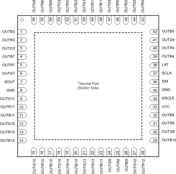
Terminal Functions
| TERMINAL | I/O | DESCRIPTION | ||
|---|---|---|---|---|
| NAME | DCA NUMBER | RTQ NUMBER | ||
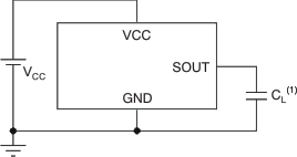
| GND | 29, 56 | 8, 35 | — | Power ground |
| GSCLK | 55 | 34 | I | Reference clock for the grayscale (GS) pulse width modulation (PWM) control for all outputs. Each GSCLK rising edge increments the grayscale counter for PWM control. When the LAT signal is input for a GS data write with the timing reset mode enabled, all constant-current outputs (OUTX0-OUTX15, where X = R, G, or B) are forced off, the grayscale counter is reset to 0, and the grayscale PWM timing controller is initialized. |
| LAT | 3 | 38 | I | The LAT rising edge either latches the data from the common shift register into the GS data latch when the MSB of the common shift register is 0 or latches the data into the control data latch when the MSB of the common shift register is 1. When the display timing reset bit (TMGRST) in the control data latch is 1, the grayscale counter initialized at the LAT signal is input for a grayscale data write. Dot correction (DC) data in the control data latch are copied to DC data latch at the same time. |
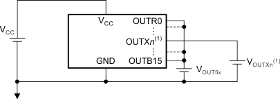
| OUTB0 to OUTB15 | 4, 7, 10, 13, 16, 19, 22, 25, 32, 35, 38, 41, 44, 47, 50, 53 | 1, 4, 11, 14, 17, 20, 23, 26, 29, 32, 39, 42, 45, 48, 51, 54 | O | Constant-current outputs for the blue color group. Multiple outputs can be configured in parallel to increase the constant-current capability. Different voltages can be applied to each output. |
| OUTG0 to OUTG15 | 6, 9, 12, 15, 18, 21, 24, 27, 30, 33, 36, 39, 42, 45, 48, 51 | 3, 6, 9, 12, 15, 18, 21, 24, 27, 30, 41, 44, 47, 50, 53, 56 | O | Constant-current outputs for the green color group. Multiple outputs can be configured in parallel to increase the constant-current capability. Different voltages can be applied to each output. |
| OUTR0 to OUTR15 | 5, 8, 11, 14, 17, 20, 23, 26, 31, 34, 37, 40, 43, 46, 49, 52 | 2, 5, 10, 13, 16, 19, 22, 25, 28, 31, 40, 43, 46, 49, 52, 55 | O | Constant-current outputs for the red color group. Multiple outputs can be configured in parallel to increase the constant-current capability. Different voltages can be applied to each output. |
| SCLK | 2 | 37 | I | Serial data shift clock. Data present on SIN are shifted to the LSB of the common shift register with the SCLK rising edge. Data in the shift register are shifted toward the MSB at each SCLK rising edge. The MSB data of the common shift register appears on SOUT. |
| SIN | 1 | 36 | I | Serial data input for the 769-bit common shift register. |
| SOUT | 28 | 7 | O | This bit is the serial data output of the 769-bit common shift register. LED open detection (LOD) and LED short detection (LSD) can be read out with SOUT in the form of status information data (SID) after the LAT falling edge is input for a GS data write. SOUT is connected to the MSB of the 769-bit common shift register. Data are clocked out at the SCLK rising edge. |
| VCC | 54 | 33 | — | Power-supply voltage |
| Thermal pad | — | The thermal pad is not connected to GND internally. The thermal pad must be connected to GND via the PCB. |
||
6 Specifications
6.1 Absolute Maximum Ratings(1)
Over operating free-air temperature range, unless otherwise noted.| MIN | MAX | UNIT | ||||
|---|---|---|---|---|---|---|
| VCC | Voltage(2) | Supply | –0.3 | +6.0 | V | |
| VIN | Input range | SIN, SCLK, LAT, GSCLK | –0.3 | VCC + 0.3 | V | |
| VOUT | Output range | SOUT | –0.3 | VCC + 0.3 | V | |
| OUTR0 to OUTR15, OUTG0 to OUTG15, OUTB0 to OUTB15 | –0.3 | +11 | V | |||
| TJ (max) | Maximum operating junction temperature | +150 | °C | |||
6.2 Handling Ratings
| MIN | MAX | UNIT | ||
|---|---|---|---|---|
| TSTG | Storage temperature range | –55 | +150 | °C |
| VESD(1) | Human body model (HBM) ESD stress voltage(2) | 4000 | V | |
| Charged device model (CDM) ESD stress voltage(3) | 2000 | V |
6.3 Recommended Operating Conditions
| PARAMETER | TEST CONDITIONS | MIN | NOM | MAX | UNIT | |
|---|---|---|---|---|---|---|
| DC CHARACTERISTICS | ||||||
| VCC | Supply voltage | 3.0 | 5.5 | V | ||
| VO | Voltage applied to output | OUTX0 to OUTX15(2) | 10 | V | ||
| VIH | High-level input voltage | SIN, SCLK, LAT, GSCLK | 0.7 × VCC | VCC | V | |
| VIL | Low-level input voltage | SIN, SCLK, LAT, GSCLK | GND | 0.3 × VCC | V | |
| IOH | High-level output current | SOUT | –2 | mA | ||
| IOL | Low-level output current | SOUT | 2 | mA | ||
| IOLC | Constant output sink current | OUTX0 to OUTX15(2), 3 V ≤ VCC ≤ 3.6 V | 23.9 | mA | ||
| OUTX0 to OUTX15(2), 3.6 V < VCC ≤ 5.5 V | 31.9 | mA | ||||
| TA | Operating free-air temperature range | –40 | +85 | °C | ||
| TJ | Operating junction temperature range | –40 | +125 | °C | ||
| AC CHARACTERISTICS | ||||||
| fCLK (SCLK) | Data shift clock frequency | SCLK | 25 | MHz | ||
| fCLK (GSCLK) | Grayscale control clock frequency | GSCLK | 33 | MHz | ||
| tWH0 | Pulse duration | SCLK | 10 | ns | ||
| tWL0 | SCLK | 10 | ns | |||
| tWH1 | GSCLK | 10 | ns | |||
| tWL1 | GSCLK | 10 | ns | |||
| tWH2 | LAT | 30 | ns | |||
| tSU0 | Setup time | SIN to SCLK↑ | 5 | ns | ||
| tSU1 | LAT↓ to SCLK↑ (auto data refresh is disabled(1)) | 30 | ns | |||
| tSU2 | LAT↑ for GS data written to GSCLK↑ when display time reset mode is disabled | 50 | ns | |||
| tSU3 | LAT↑ for GS data written to GSCLK↑ when display time reset mode is enabled | 70 | ns | |||
| tH0 | Hold time | SCLK↑ to SIN | 2 | ns | ||
| tH1 | SCLK↑ to LAT↑ | 5 | ns | |||
6.4 Thermal Information
| THERMAL METRIC(1) | DCA (HTSSOP) | RTQ (QFN) | UNIT | |
|---|---|---|---|---|
| 56 TERMINALS | 56 TERMINALS | |||
| θJA | Junction-to-ambient thermal resistance | 32.2 | 27.9 | °C/W |
| θJCtop | Junction-to-case (top) thermal resistance | 16.8 | 14.9 | |
| θJB | Junction-to-board thermal resistance | 16.1 | 6.5 | |
| ψJT | Junction-to-top characterization parameter | 0.8 | 0.3 | |
| ψJB | Junction-to-board characterization parameter | 16.0 | 6.4 | |
| θJCbot | Junction-to-case (bottom) thermal resistance | 0.9 | 2.0 | |
6.5 Electrical Characteristics
At TA = –40°C to +85°C and VCC = 3 V to 5.5 V, unless otherwise noted. Typical values at TA = +25°C and VCC = 3.3 V.| PARAMETER | CONDITION | MIN | TYP | MAX | UNIT | ||
|---|---|---|---|---|---|---|---|
| VOH | High-level output voltage (SOUT) | IOH = –2 mA | VCC – 0.4 | VCC | V | ||
| VOL | Low-level output voltage (SOUT) | IOL = 2 mA | 0.4 | V | |||
| IIN | Input current (SIN, SCLK, LAT, GSCLK) |
VIN = VCC or GND | –1 | 1 | μA | ||
| ICC0 | Supply current (VCC) | SIN, SCLK, and LAT = GND, all OUTXn = off, GSCLK = GND, GSXn = 0000h, DCXn and BCX = 7Fh, VOUTXn = 0.8 V, MCX = 0 (3.2-mA target)(1)(2) |
15 | 20 | mA | ||
| ICC1 | SIN, SCLK, and LAT = GND, all OUTXn = off, GSCLK = GND, GSXn = 0000h, DCXn and BCX = 7Fh, VOUTXn = 0.8 V, MCX = 4 (19.1-mA target) |
16 | 22 | mA | |||
| ICC2 | SIN, SCLK, and LAT = GND, auto display repeat enabled, GSCLK = 33 MHz, GSXn = FFFFh, DCXn and BCX = 7Fh, VOUTXn = 0.8 V, MCX = 4 (19.1-mA target) | 18 | 26 | mA | |||
| ICC3 | VCC = 5.0 V, SIN, SCLK, and LAT = GND, auto display repeat enabled, GSCLK = 33 MHz, GSXn = FFFFh, DCXn and BCX = 7Fh, VOUTXn = 0.8 V, MCX = 7 (31.9-mA target) |
20 | 29 | mA | |||
| IOLC0 | Constant output sink current (OUTX0 to OUTX15) |
All OUTXn = on, DCXn and BCX = 7Fh, VOUTXn = VOUTfix = 0.8 V, MCX = 4 |
17.4 | 19.1 | 20.8 | mA | |
| IOLC1 | VCC = 5.0 V, all OUTXn = on, DCXn and BCX = 7Fh, VOUTXn = VOUTfix = 0.8 V, MCX = 7 | 29.1 | 31.9 | 34.7 | mA | ||
| IOLKG0 | Output leakage current (OUTX0 to OUTX15) |
All OUTn = off, VOUTXn = VOUTfix = 10 V, MCX = 7 |
TJ = +25°C | 0.1 | μA | ||
| IOLKG1 | TJ = +85°C | 0.2 | μA | ||||
| IOLKG2 | TJ = +125°C | 0.3 | 0.8 | μA | |||
| ΔIOLC0 | Constant-current error (channel-to-channel, OUTX0 to OUTX15)(3) |
All OUTXn = on, DCXn and BCX = 7Fh, VOUTXn = VOUTfix = 0.8 V, MCX = 4 |
±2% | ±5% | |||
| ΔIOLC1 | Constant-current error (device-to-device, OUTX0 to OUTX15)(4) |
All OUTXn = on, DCXn and BCX = 7Fh, VOUTXn = VOUTfix = 0.8 V, MCX = 4 |
±2% | ±4% | |||
| ΔIOLC2 | Line regulation (OUTx0 to OUTx15)(5) |
VCC = 3.0 V to 5.5 V, all OUTXn = on, DCXn and BCX = 7Fh, VOUTXn = VOUTfix = 0.8 V, MCX = 4 |
±0.1 | ±1 | %/V | ||
| ΔIOLC3 | Load regulation (OUTx0 to OUTx15)(6) |
All OUTXn = on, DCXn and BCX = 7Fh, VOUTXn = 0.8 V to 3.0 V, VOUTfix = 0.8 V, MCX = 4 |
±0.1 | ±1 | %/V | ||
| VLOD | LED open-detection threshold | All OUTXn = on | 0.25 | 0.30 | 0.35 | V | |
| VLSD0 | LED short-detection threshold | All OUTXn = on, LSDVLT = 0 | 0.65 × VCC | 0.70 × VCC | 0.75 × VCC | V | |
| VLSD1 | All OUTXn = on, LSDVLT = 1 | 0.85 × VCC | 0.90 × VCC | 0.95 × VCC | V | ||

where X = R, G, or B; n = 0 to 15.
Deviation is calculated by the formula:

where X = R, G, or B; n = 0 to 15.
Ideal current is the target current when MC is 4.

where X = R, G, or B; n = 0 to 15.
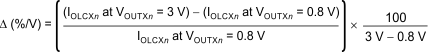
where X = R, G, or B; n = 0 to 15.
6.6 Switching Characteristics
At TA = –40°C to +85°C, VCC = 3 V to 5.5 V, CL = 15 pF, RL = 120 Ω, MCX = 7, and VLED = 4.5 V, unless otherwise noted. Typical values at TA = +25°C and VCC = 3.3 V.| PARAMETER | TEST CONDITIONS | MIN | TYP | MAX | UNIT | ||
|---|---|---|---|---|---|---|---|
| tR0 | Rise time | SOUT | 3 | 5 | ns | ||
| tR1 | OUTXn, VCC = 3.6 V, DCXn, and BCX = 7Fh, TA = +25°C(2) | 30 | ns | ||||
| tF0 | Fall time | SOUT | 3 | 5 | ns | ||
| tF1 | OUTXn, VCC = 3.6 V, DCXn, and BCX = 7Fh, TA = +25°C | 40 | ns | ||||
| tD0 | Propagation delay | SCLK↑ to SOUT↑↓ | 20 | 30 | ns | ||
| tD1 | VCC = 3.6 V, GSCLK = 33 MHz, DCXn and BCX = 7Fh, TA = +25°C | GSCLK↑ to OUTX4 and OUTX11 on or off |
40 | ns | |||
| tD2 | GSCLK↑ to OUTX0 and OUTX15 on or off |
43 | ns | ||||
| tD3 | GSCLK↑ to OUTX5 and OUTX10 on or off |
46 | ns | ||||
| tD4 | GSCLK↑ to OUTX1 and OUTX14 on or off |
49 | ns | ||||
| tD5 | GSCLK↑ to OUTX2 and OUTX13 on or off |
52 | ns | ||||
| tD6 | GSCLK↑ to OUTX6 and OUTX9 on or off |
55 | ns | ||||
| tD7 | GSCLK↑ to OUTX3 and OUTX12 on or off |
58 | ns | ||||
| tD8 | GSCLK↑ to OUTX7 and OUTX8 on or off |
61 | ns | ||||
| tON_ERR | Output on-time error(1) | tOUTON – tGSCLK, VCC = 3.6 V to 5.5 V, GSXn = 0001h, GSCLK = 33 MHz, DCXn and BCX = 7Fh |
–20 | 20 | ns | ||
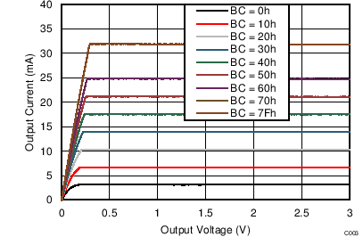
6.7 Typical Characteristics
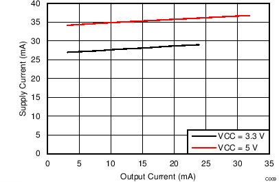
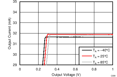
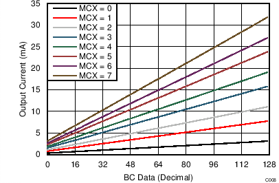
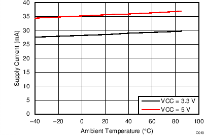
At TA = +25°C and VCC = 5.0 V, unless otherwise noted.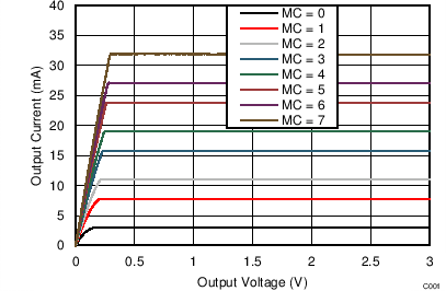
| BCX = DCXn = 7Fh |
(MCX Changing)
| BCX = DCXn = 7Fh |
(BCX Changing)

| BCX = DCXn = 7Fh | VOUTXn = 0.8 V | |

| BCX = 7Fh | VOUTXn = 0.8 V | |
| BCX = DCXn = 7Fh | SIN = 12.5 MHz | SCLK = 25 MHz |
| GSCLK = 33 MHz | VOUT = 0.8 V | GSXn = FFFFh |

| MCX = 7 | BCX = DCXn = 7Fh | GSCLK = 33 MHz | |||
| VLED = 4.5 V | RL = 120 Ω | GSXn = 0001h | |||

| BCX = DCXn = 7Fh |
(DCXn Changing)
| BCX = DCXn = 7Fh |

| MCX = 4 | BCX = DCXn = 7Fh | VOUTXn = 0.8 V |
| DCXn = 7Fh | VOUTXn = 0.8 V | |
| MCX = 4 | BCX = DCXn = 7Fh | SIN = 12.5 MHz |
| SCLK = 25 MHz | GSCLK = 33 MHz | VOUT = 0.8 V |
| GSXn = FFFFh |
7 Parameter Measurement Information
7.1 Terminal-Equivalent Input and Output Schematic Diagrams
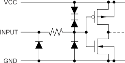 Figure 12. SIN, SCLK, LAT, GSCLK
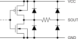 Figure 13. SOUT
7.2 Test Circuits
7.3 Timing Diagrams
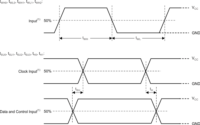
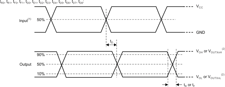
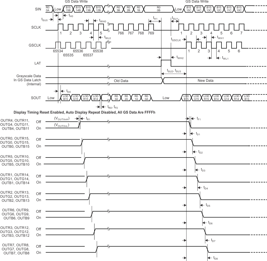 Figure 20. Data Input, Output, and Constant Output Timing