JAJSJ97C July 2020 – March 2022 TLIN2027-Q1
PRODUCTION DATA
- 1 特長
- 2 アプリケーション
- 3 概要
- 4 Revision History
- 5 概要 (続き)
- 6 Pin Configuration and Functions
- 7 Specifications
- 8 Parameter Measurement Information
-
9 Detailed Description
- 9.1 Overview
- 9.2 Functional Block Diagram
- 9.3
Feature Description
- 9.3.1 LIN (Local Interconnect Network) Bus
- 9.3.2 TXD (Transmit Input and Output)
- 9.3.3 RXD (Receive Output)
- 9.3.4 VSUP (Supply Voltage)
- 9.3.5 GND (Ground)
- 9.3.6 EN (Enable Input)
- 9.3.7 Protection Features
- 9.3.8 Bus Stuck Dominant System Fault: False Wake-Up Lockout
- 9.3.9 Thermal Shutdown
- 9.3.10 Under Voltage on VSUP
- 9.3.11 Unpowered Device and LIN Bus
- 9.4 Device Functional Modes
- 10Application and Implementation
- 11Power Supply Recommendations
- 12Layout
- 13Device and Documentation Support
- 14Mechanical, Packaging, and Orderable Information
パッケージ・オプション
メカニカル・データ(パッケージ|ピン)
サーマルパッド・メカニカル・データ
- DRB|8
発注情報
6 Pin Configuration and Functions
Figure 6-1 D Package, 8-Pin (SOIC),
Top View
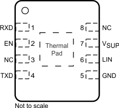
 Figure 6-2 DRB Package, 8-Pin (VSON),
Top View
Figure 6-2 DRB Package, 8-Pin (VSON),
Top ViewTable 6-1 Pin Functions
| PIN | Type | DESCRIPTION | |
|---|---|---|---|
| Name | No. | ||
| RXD | 1 | DO | RXD output (open-drain) interface reporting state of LIN bus voltage |
| EN | 2 | DI | Enable input - High puts the device in normal operation mode and low puts the device in sleep mode |
| NC | 3 | – | Not connected |
| TXD | 4 | DI | TXD input interface to control state of LIN output - Internally pulled to ground |
| GND | 5 | GND | Ground |
| LIN | 6 | HV I/O | LIN bus single-wire transmitter and receiver |
| VSUP | 7 | HV Supply | Device supply voltage (connected to battery in series with external reverse blocking diode) |
| NC | 8 | – | Not connected |
| Thermal Pad | - | No electrical connection. Can be connected to the PCB to improve thermal coupling (DRB package only) | |