JAJSGQ8C December   2018  – June 2022 TLIN2441-Q1

PRODUCTION DATA  

  1. 特長
  2. アプリケーション
  3. 概要
  4. Revision History
  5. 概要 (続き)
  6. Pin Configuration and Functions
  7. Specifications
    1. 7.1 Absolute Maximum Ratings
    2. 7.2 ESD Ratings
    3. 7.3 ESD Ratings, IEC Specification
    4. 7.4 Recommended Operating Conditions
    5. 7.5 Thermal Information
    6. 7.6 Power Supply Characteristics
    7. 7.7 Electrical Characteristics
    8. 7.8 AC Switching Characteristics
    9. 7.9 Typical Characteristics
  8. Parameter Measurement Information
    1. 8.1 Test Circuit: Diagrams and Waveforms
  9. Detailed Description
    1. 9.1 Overview
    2. 9.2 Functional Block Diagram
    3. 9.3 Feature Description
      1. 9.3.1  LIN Pin
        1. 9.3.1.1 LIN Transmitter Characteristics
        2. 9.3.1.2 LIN Receiver Characteristics
          1. 9.3.1.2.1 Termination
      2. 9.3.2  TXD (Transmit Input)
      3. 9.3.3  RXD (Receive Output)
      4. 9.3.4  WAKE (High Voltage Local Wake Up Input)
      5. 9.3.5  WDT/CLK (Pin Programmable Watchdog Delay Input/SPI Clock)
      6. 9.3.6  WDI/SDI (Watchdog Timer Input/SPI Serial Data In)
      7. 9.3.7  PIN/nCS (Pin Watchdog Select/SPI Chip Select)
      8. 9.3.8  LIMP (LIMP Home output – High Voltage Open Drain Output)
      9. 9.3.9  nWDR/SDO (Watchdog Timeout Reset Output/SPI Serial Data Out)
      10. 9.3.10 VSUP (Supply Voltage)
      11. 9.3.11 GND (Ground)
      12. 9.3.12 EN/nINT (Enable Input/Interrupt Output in SPI Mode)
      13. 9.3.13 nRST/nWDR (Reset Output/Watchdog Timeout Reset Output)
      14. 9.3.14 VCC (Supply Output)
      15. 9.3.15 Protection Features
        1. 9.3.15.1 TXD Dominant Time Out (DTO)
        2. 9.3.15.2 Bus Stuck Dominant System Fault: False Wake Up Lockout
        3. 9.3.15.3 Thermal Shutdown
        4. 9.3.15.4 Under Voltage on VSUP
        5. 9.3.15.5 Unpowered Device and LIN Bus
    4. 9.4 Device Functional Modes
      1. 9.4.1 Normal Mode
      2. 9.4.2 Sleep Mode
      3. 9.4.3 Standby Mode
      4. 9.4.4 Failsafe Mode
      5. 9.4.5 Wake-Up Events
        1. 9.4.5.1 Wake-Up Request (RXD)
        2. 9.4.5.2 Local Wake Up (LWU) via WAKE Terminal
      6. 9.4.6 Mode Transitions
      7. 9.4.7 Voltage Regulator
        1. 9.4.7.1 VCC
        2. 9.4.7.2 Output Capacitance Selection
        3. 9.4.7.3 Low-Voltage Tracking
        4. 9.4.7.4 Power Supply Recommendation
      8. 9.4.8 Watchdog
        1. 9.4.8.1 Watchdog Error Counter
        2. 9.4.8.2 Pin Control Mode
        3. 9.4.8.3 SPI Control Programming
        4. 9.4.8.4 Watchdog Timing
    5. 9.5 Programming
      1. 9.5.1 SPI Communication
        1. 9.5.1.1 Chip Select Not (nCS)
        2. 9.5.1.2 Serial Clock Input (CLK)
        3. 9.5.1.3 Serial Data Input (SDI)
        4. 9.5.1.4 Serial Data Output (SDO)
    6. 9.6 Registers
  10. 10Application and Implementation
    1. 10.1 Application Information
    2. 10.2 Typical Application
      1. 10.2.1 Design Requirements
        1. 10.2.1.1 Normal Mode Application Note
        2. 10.2.1.2 Standby Mode Application Note
        3. 10.2.1.3 TXD Dominant State Timeout Application Note
      2. 10.2.2 Detailed Design Procedures
      3. 10.2.3 Application Curves
  11. 11Power Supply Recommendations
  12. 12Layout
    1. 12.1 Layout Guidelines
    2. 12.2 Layout Example
  13. 13Device and Documentation Support
    1. 13.1 Documentation Support
      1. 13.1.1 Related Documentation
    2. 13.2 Receiving Notification of Documentation Updates
    3. 13.3 サポート・リソース
    4. 13.4 Trademarks
    5. 13.5 Electrostatic Discharge Caution
    6. 13.6 Glossary
  14. 14Mechanical, Packaging, and Orderable Information

パッケージ・オプション

メカニカル・データ(パッケージ|ピン)
サーマルパッド・メカニカル・データ
発注情報

Local Wake Up (LWU) via WAKE Terminal

The WAKE terminal is a high voltage input terminal which can be used for local wake up (LWU) request via a voltage transition. The terminal triggers a LWU event on a high to low or low to high transition. This terminal may be used with a switch to ground or VSUP. If the terminal is not used, it should be connected to VSUP to avoid unwanted parasitic wake up.

The LWU circuitry is active in sleep mode and standby mode. If a valid LWU event occurs, the device transitions to standby mode. The LWU circuitry is not active in normal mode. To minimize system level current consumption, the internal bias voltages of the terminal follows the state on the terminal with a delay of tWAKE(MIN). A constant high level on WAKE has an internal pull up to VSUP and a constant low level on WAKE has an internal pull-down to ground. On power up, this may look like a LWU event and could be flagged as such.
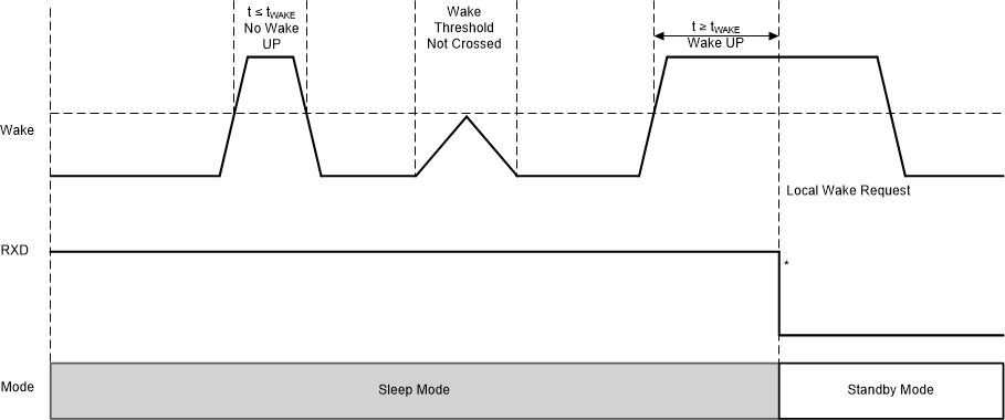
GUID-8A0402A2-685D-4544-BECE-550DB8F98E85-low.gifFigure 9-8 Local Wake Up (LWU) - Rising Edge
GUID-1151D562-1A6E-4C66-A054-6062D9403D91-low.gifFigure 9-9 Local Wake Up (LWU) - Falling Edge