SLLSEC7A August 2012 – October 2015 TLK10034
PRODUCTION DATA.
- 1Device Overview
- 2Revision History
- 3Pin Configuration and Functions
-
4Specifications
- 4.1 Absolute Maximum Ratings
- 4.2 ESD Ratings
- 4.3 Recommended Operating Conditions
- 4.4 Thermal Information
- 4.5 LVCMOS Electrical Characteristics (VDDO)
- 4.6 High Speed Side Serial Transmitter Characteristics
- 4.7 High Speed Side Serial Receiver Characteristics
- 4.8 Low Speed Side Serial Transmitter Characteristics
- 4.9 Low Speed Side Serial Receiver Characteristics
- 4.10 Reference Clock Characteristics (REFCLK0P/N, REFCLK1P/N)
- 4.11 Differential Output Clock Characteristics (CLKOUTA/B/C/DP/N)
- 4.12 MDIO Timing Requirements
- 4.13 JTAG Timing Requirements
- 4.14 Typical Characteristics
-
5Detailed Description
- 5.1 Overview
- 5.2 Functional Block Diagrams
- 5.3
Feature Description
- 5.3.1
10GBASE-KR Mode
- 5.3.1.1 10GBASE-KR Transmit Data Path Overview
- 5.3.1.2 10GBASE-KR Receive Data Path Overview
- 5.3.1.3 Channel Synchronization Block
- 5.3.1.4 8B/10B Encoder
- 5.3.1.5 8B/10B Decoder
- 5.3.1.6 64B/66B Encoder/Scrambler
- 5.3.1.7 64B/66B Decoder/Descrambler
- 5.3.1.8 Transmit Gearbox
- 5.3.1.9 Receive Gearbox
- 5.3.1.10 XAUI Lane Alignment / Code Gen (XAUI PCS)
- 5.3.1.11 XAUI Inter-Packet Gap (IPG) Handling
- 5.3.1.12 Clock Tolerance Compensation (CTC)
- 5.3.1.13 10GBASE-KR Auto-Negotiation
- 5.3.1.14 10GBASE-KR Link Training
- 5.3.1.15 Forward Error Correction
- 5.3.1.16 10GBASE-KR Line Rate, PLL Settings, and Reference Clock Selection
- 5.3.1.17 10GBASE-KR Loopback Modes
- 5.3.1.18 10GBASE-KR Test Pattern Support
- 5.3.1.19 10GBASE-KR Latency
- 5.3.2 1GBASE-KX Mode
- 5.3.3
General Purpose (10G) SerDes Mode
- 5.3.3.1 General Purpose SERDES Transmit Data Path
- 5.3.3.2 General Purpose SERDES Receive Data Path
- 5.3.3.3 Channel Synchronization
- 5.3.3.4 8B/10B Encoder and Decoder
- 5.3.3.5 Lane Alignment Scheme for 8b/10b General Purpose Serdes Mode (Non XAUI Fata, - No /A/)
- 5.3.3.6 Lane Alignment Components
- 5.3.3.7 Lane Alignment Operation (General Purpose Serdes Mode)
- 5.3.3.8 Line Rate, SERDES PLL Settings, and Reference Clock Selection for the General Purpose SERDES Mode
- 5.3.3.9 General Purpose (10G) Loopback Modes
- 5.3.3.10 General Purpose (10G) Latency Measurement Function
- 5.3.3.11 General Purpose (10G) Mode Latency
- 5.3.3.12 TLK10034 Clocks: REFCLK, CLKOUT
- 5.3.3.13 TLK10034 Control Pins and Interfaces
- 5.3.3.14 MDIO Interface
- 5.3.3.15 JTAG Interface
- 5.3.3.16 Unused Pins
- 5.3.4 Provisionable XAUI Clock Tolerance Compensation
- 5.3.1
10GBASE-KR Mode
- 5.4 Device Functional Modes
- 5.5 Memory
- 5.6 Register Map
- 6Application and Implementation
- 7Device and Documentation Support
- 8Mechanical, Packaging, and Orderable Information
6 Application and Implementation
NOTE
Information in the following applications sections is not part of the TI component specification, and TI does not warrant its accuracy or completeness. TI’s customers are responsible for determining suitability of components for their purposes. Customers should validate and test their design implementation to confirm system functionality.
6.1 Application Information
Each channel of the TLK10034 can be used to convert between XAUI (on the low speed port) and 10GBASE-R signaling (on the high speed port). The high speed side of the device meets the requirements of the 10GBASE-KR physical layer standard for 10 Gbps data transmission over a PCB backplane. The device can also be used for optical physical layers (like 10GBASE-SR or 10GBASE-LR) by interfacing to optical modules requiring SFI or XFI electrical signaling. For optical use cases, KR-specific features like Clause 73 auto-negotiation and link training should be disabled.
6.2 Typical Application
A typical application for TLK10034 is to support 10 Gbps Ethernet data transmission over a backplane, e.g., between a network processor or MAC and switch ASIC located on separate cards within a router chassis. A block diagram of this application is shown below.
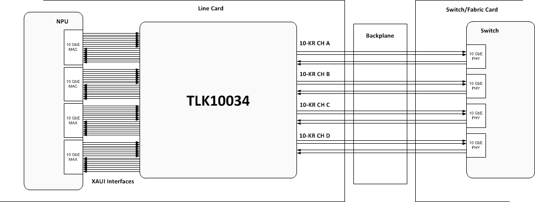 Figure 6-1 Typical Application Circuit
6.2.1 Design Requirements
Table 6-1 lists the design requirements for this typical application example.
Table 6-1 Design Parameters
| PARAMETER | VALUE |
|---|---|
| 10GBASE-KR Interface Requirements | |
| Signaling rate | 10.3125 Gbps, ±100ppm |
| Differential peak-to-peak output voltage (maximum) | 1200 mV |
| Total jitter (maximum) | 0.28 UI |
| Encoding | 64b/66b |
| Scrambling | Yes |
| Auto-negotiation? | Yes |
| Link training | Yes |
| XAUI Interface Requirements | |
| Signaling rate per lane | 3.125 Gbps ±100 ppm |
| Differential peak-to-peak output voltage (maximum) | 1600 mV |
| Total jitter (maximum) | 0.35 UI |
| Encoding | 8b/10b |
6.2.2 Detailed Design Procedure
The TLK10034 should be powered via a 1-V (nominal) supply on the VDDD, VDDA, DVDD, VDDT, and VPP rails and by a 1.5-V or 1.8-V (nominal) supply on the VDDR and VDDO rails. The power supply accuracy should be 5% or better, and the user should be careful that resistive losses across the application PCB’s power distribution network do not cause the voltage present at the TLK10034’s BGA balls to be below specification. If a switched-mode power supply is used, care should be taken to ensure low supply ripple.
A differential reference clock must be provided to either the REFCLK0P/N or REFCLK1P/N input port. The clock signal should be AC-coupled and have a differential amplitude between 250 mV and 2000 mV peak-to-peak. For 10GBASE-R applications, the clock frequency should be either 156.25 MHz or 312.5 MHz and have an accuracy of 100 ppm. Because jitter on the reference clock can transfer through the TLK10034’s PLLs and onto the serial outputs, it is best to keep the reference clock’s jitter as low as possible (e.g., under 1 ps from 10 kHz to 20 MHz) in order to meet the requirements of IEEE 802.3.
All serial inputs and outputs should be laid out on the PCB following best practices for high speed signal integrity. Detailed layout recommendations are given in the Section 6.2.4.1 section.
6.2.3 Application Curve
The output eye diagram of the TLK10034 (operated at 10.3125 Gbps under nominal conditions) is shown below.
 Figure 6-2 Eye Diagram of the TLK10034
6.2.4 Layout
6.2.4.1 Layout Guidelines
6.2.4.1.1 TLK10034 High-Speed Data Path
Both “low-speed” side and “high-speed” side serial signals are referred to as “high-speed” signals for the purpose of this document as they support very high data rates. For that reason care must be taken to realize them on a printed circuit board with signal integrity in mind. The high-speed data path CML input pins INA[3:0]P/INA[3:0]N, INB[3:0]P/INB[3:0]N, HSRXAP/HSRXAN, and HSRXBP/HSRXBN, and the CML output pins OUTA[3:0]P/OUTA[3:0]N, OUTB[3:0]P/OUTB[3:0]N, HSTXAP/HSTXAN, and HSTXBP/HSTXBN, have to be connected with loosely-coupled 100-Ω differential transmission lines. Differential intra-pair skew needs to be minimized to within ±1 mil. Inter-pair (lane-to-lane) skew for the low-speed signals can be as high as 30 UI. An example of FR-4 printed circuit board (PCB) realization of such differential transmission lines in microstrip format is shown in Figure 6-8.
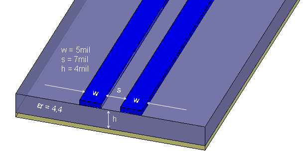 Figure 6-3 Differential Microstrip PCB Trace Geometry Example
To avoid impedance discontinuities the high-speed serial signals should be routed on a PCB on either the top or bottom PCB layers in microstrip format with no VIAS. If VIAS are unavoidable, an absolute minimum number of vias need to be used. The VIAS should be made to stretch through the entire PCB thickness (as shown in Figure 12-2) to connect microstrip traces on the top and bottom layers of the PCB so as to leave no via stubs that can severely impact the performance. If stripline traces are absolutely necessary, and if via back-drilling is not possible, then the routing layers should be chosen so as to have via stubs that are shorter than 10 mils.
All unused internal layer via pads on high-speed signal VIAS should be removed to further improve impedance matching. On the high-speed side, the HSRXAP/HSRXAN and HSRXBP/HSRXBN signals are more sensitive to impedance discontinuities introduced by VIAS than HSTXAP/HSTXAN and HSTXBP/HSTXBN signals. For that reason, if only some of those signals need to be routed with VIAS, then the latter should be routed with VIAS and the former with no VIAS.
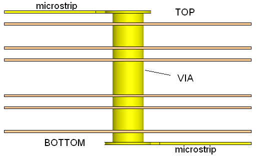
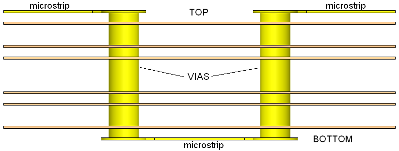 Figure 6-4 Examples of High-Speed PCB Traces with VIAS that Have No Via Stubs and No Via Pads on Internal Layers
To further improve on impedance matching, differential vias with neighboring ground vias can be used as shown in Figure 6-5. The optimum dimensions of such a differential via structure depend on various parameters such as the trace geometry, dielectric material, as well as the PCB layer stack-up. A 3D electromagnetic field solver can be used to find the optimum via dimensions.
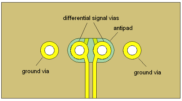 Figure 6-5 A Differential PCB via Structure (Top View)
PCB traces connected to the HSRXAP/HSRXAN and HSRXBP/HSRXBN pins should have differential insertion loss of less than 25 dB at 5 GHz.
Surface-mount connector pads such as those used with the SFP/SFP+ module connectors are wider and hence have characteristic impedance that is lower than the regular high-speed PCB traces. If the pads are more than 2 times wider than the PCB traces, the pads’ impedance needs to be increased to minimize impedance discontinuities. The easy way of increasing the pads’ impedance is to cut out the reference plane immediately under those pads as shown in Figure 6-6 so as to have the pads refer to a reference plane on lower layers while maintaining 100Ω differential characteristic impedance.
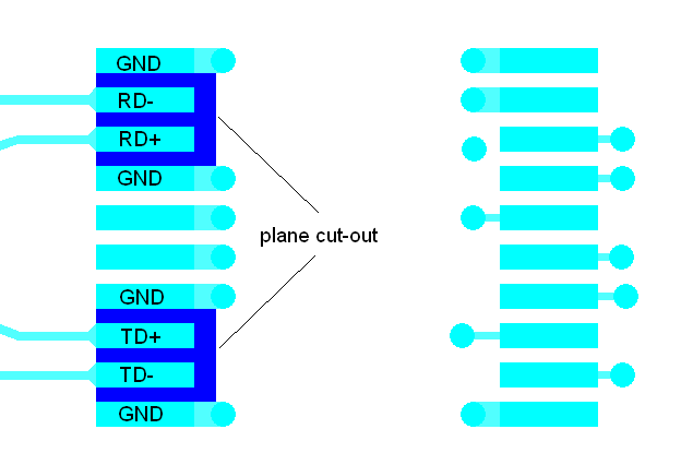 Figure 6-6 Reference Plane Cut-Out Under SFP/SFP+ Module Connector Pads
6.2.4.1.2 AC-Coupling
A 0.1-uF series AC-coupling capacitor should be connected to each of the high-speed data path pins INA[3:0]P/INA[3:0]N, INB[3:0]P/INB[3:0]N, HSRXAP/HSRXAN, HSRXBP/HSRXBN,
OUTA[3:0]P/OUTA[3:0]N, OUTB[3:0]P/OUTB[3:0]N, HSTXAP/HSTXAN, and HSTXBP/HSTXBN. If the TLK10034 high-speed side data path pins are connected to SFP/SFP+ optical modules with internal AC-coupling capacitors, then no external capacitors should be used. Adding additional series capacitors may severely impact the performance.
To avoid impedance discontinuities, it is strongly recommended where possible to make the transmission line trace width closely match the AC-coupling capacitor pad size. Smaller capacitor packages such as 0201 make it easy to meet that condition.
6.2.4.1.3 External Clock Connections
An external clock jitter cleaner, such as Texas Instruments CDCE72010 or CDCM7005, may be used when needed to provide a low jitter reference clock. An example external clock jitter cleaner connection for channel A is shown in Figure 6-7.
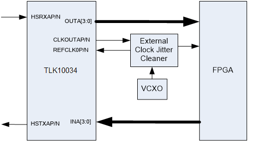 Figure 6-7 External Clock Jitter Cleaner Connection Example for Channel A
6.2.4.2 Layout Example
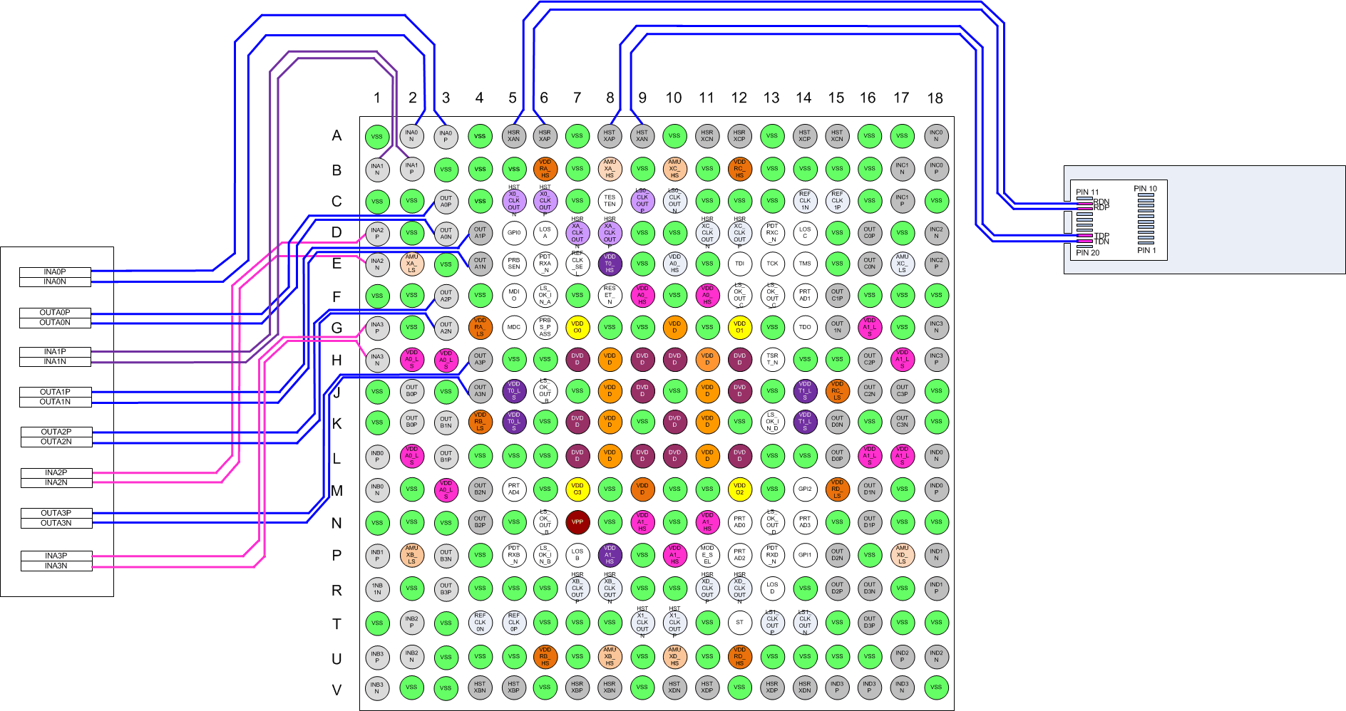 Figure 6-8 TLK10034 Pinout and Routing
6.2.4.3 Package Thermal Dissipation Ratings
Table 6-2 details the thermal characteristics of the TLK10034 package.
Table 6-2 Package Thermal Characteristics
| JEDEC STANDARD BOARD | ||
|---|---|---|
| PARAMETER | VALUE | |
| ΘJA | Theta-JA | 21.2°C/W |
| ΨJT | Psi-JT | 0.10°C/W |
| ΨJB | Psi-JB | 7.7°C/W |
| CUSTOM TYPICAL APPLICATION BOARD(1) | ||
| ΘJA | Theta-JA | 11.2°C/W |
| ΨJT | Psi-JT | 0.10°C/W |
| ΨJB | Psi-JB | 5.53°C/W |
- 10x15 inches
- 12 layer
- 8 power/ground layers – 95% copper (1oz)
- 4 signal layers – 20% copper (1oz)
ΨJB = (TJ – TB)/(Total Device Power Dissipation)
ΨJB = (TJ TJ = Device Junction Temperature
ΨJB = (TJ TB = Temperature of PCB 1 mm from device edge.
ΨJT = (TJ – TC)/(Total Device Power Dissipation)
ΨJB = (TJ TJ = Device Junction Temperature
ΨJB = (TJ TC = Hottest temperature on the case of the package.
6.3 Power Supply Recommendations
The TLK10034 allows either the core or I/O power supply to be powered up for an indefinite period of time while the other supply is not powered up, if all of the following conditions are met:
- All maximum ratings and recommending operating conditions are followed.
- Bus contention while 1.5/1.8V power is applied (>0V) must be limited to 100 hours over the projected lifetime of the device.
- Junction temperature is less than 105°C during device operation
NOTE
Voltage stress up to the absolute maximum voltage values for up to 100 hours of lifetime operation at a TJ of 105°C or lower will minimally impact reliability.
The TLK10034 inputs are not failsafe (i.e. cannot be driven with the I/O power disabled). TLK10034 inputs should not be driven high until their associated power supply is active.