9 Electrical Specifications
All parameters are derived by test, statistical analysis, or design.
9.1 Absolute Maximum Ratings(1)
|
|
MIN |
MAX |
UNIT |
| VDD_IO, AVDD33 |
Supply voltage |
–0.3 |
3.8 |
V |
| PFBIN1, PFBIN2 |
–0.3 |
1.8 |
| XI |
DC Input voltage |
–0.3 |
3.8 |
V |
| TD-, TD+, RD-, RD+ |
–0.3 |
6 |
| Other Inputs |
–0.3 |
3.8 |
| XO |
DC Output voltage |
–0.3 |
3.8 |
V |
| Other outputs |
–0.3 |
3.8 |
| TJ |
Maximum die temperature |
|
125 |
°C |
(1) Stresses beyond those listed under Absolute Maximum Ratings may cause permanent damage to the device. These are stress ratings only, and functional operation of the device at these or any other conditions beyond those indicated under Recommended Operating conditions is not implied. Exposure to absolute-maximum-rated conditions for extended periods may affect device reliability.
9.2 Handling Ratings
|
MIN |
MAX |
UNIT |
| Tstg |
Storage temperature range |
–65 |
150 |
°C |
| VESD |
Electrostatic discharge (ESD) performance: |
Human Body Model (HBM), per ANSI/ESDA/JEDEC JS001(1) |
All pins(3) |
–4 |
4 |
kV |
| Ethernet network pins (TD+, TD–, RD+, RD–)(5) |
–16 |
16 |
Charged Device Model (CDM),
per JESD22-C101(2) |
All pins(4) |
–750 |
750 |
V |
(1) JEDEC document JEP155 states that 500-V HBM allows safe manufacturing with a standard ESD control process.
(2) JEDEC document JEP157 states that 250-V CDM allows safe manufacturing with a standard ESD control process.
(3) Tested in accordance to JEDEC Standard 22, Test Method A114.
(4) Tested in accordance to JEDEC Standard 22, Test Method C101.
(5) Test method based upon JEDEC Standard 22 Test Method A114, Ethernet network pins (TD+, TD–, RD+, RD–) pins stressed with respect to GND.
9.3 Recommended Operating Conditions
|
MIN |
NOM |
MAX |
UNIT |
| DUAL SUPPLY OPERATION |
|
Core Supply voltage (PFBIN1, PFBIN2) |
1.48 |
1.55 |
1.68 |
V |
| PD |
Power dissipation(2) |
|
200 |
|
mW |
| SINGLE SUPPLY OPERATION |
|
(PFBOUT connected to PFBIN1, PFBIN2 See Figure 3-1) |
|
|
|
|
| PD |
Power dissipation(1) |
|
270 |
|
mW |
| AVDD33 |
Analog 3.3-V Supply |
3.0 |
3.3 |
3.6 |
V |
| VDD_IO |
3.3-V Option |
3.0 |
3.3 |
3.6 |
V |
| 2.5-V Option |
2.25 |
2.5 |
2.75 |
| 1.8-V Option (MII Mode only) |
1.62 |
1.8 |
1.98 |
| TA |
Ambient temperature(3) |
TLK111PT |
–40 |
|
85 |
°C |
| TLK111PTB |
–40 |
|
125 |
(1) For 100Base-TX, When internal 1.55 V is used. Device is operated from single 3.3-V supply only.
(2) For 100Base-TX
9.4 48-Pin Industrial Device Thermal Characteristics
over operating free-air temperature range (unless otherwise noted)
| THERMAL METRIC |
MIN |
TYP |
MAX |
UNIT |
| RθJA |
Junction-to-ambient thermal resistance (no airflow), JEDEC high-K model |
|
65.3 |
|
°C/W |
| RθJB |
Junction-to-board thermal resistance |
|
28.5 |
|
| RθJC |
Junction-to-case thermal resistance |
|
23.1 |
|
9.5 48-Pin Extended Temperature (125°C) Device Thermal Characteristics
over operating free-air temperature range (unless otherwise noted)
| THERMAL METRIC |
MIN |
TYP |
MAX |
UNIT |
| RθJA |
Junction-to-ambient thermal resistance (no airflow), JEDEC high-K model |
|
41.8 |
|
°C/W |
| RθJB |
Junction-to-board thermal resistance |
|
20.0 |
|
| RθJC |
Junction-to-case thermal resistance |
|
24.7 |
|
9.6 DC Characteristics, VDD_IO
over operating free-air temperature range (unless otherwise noted)
| PARAMETER |
TEST CONDITIONS |
MIN |
TYP |
MAX |
UNIT |
| 3.3V VDD_IO |
| VIH |
Input high voltage |
Nominal VCC = 3.3V |
VDD_IO = 3.3 V ±10% |
2.0 |
|
|
V |
| VIL |
Input low voltage |
|
VDD_IO = 3.3 V±10% |
|
|
0.8 |
V |
| VOL |
Output low voltage |
IOL = 4 mA |
VDD_IO = 3.3 V±10% |
|
|
0.4 |
V |
| VOH |
Output high voltage |
IOH = –4 mA |
VDD_IO = 3.3 V±10% |
VDD_IO – 0.5 |
|
|
V |
| 2.5V VDD_IO |
| VIH |
Input high voltage |
|
VDD_IO = 2.5 V±10% |
1.5 |
|
|
V |
| VIL |
Input low voltage |
|
VDD_IO = 2.5 V±10% |
|
|
0.5 |
V |
| VOL |
Output low voltage |
IOL = 2 mA |
VDD_IO = 2.5 V±10% |
|
|
0.4 |
V |
| VOH |
Output high voltage |
IOH = –2 mA |
VDD_IO = 2.5 V±10% |
VDD_IO – 0.4 |
|
|
V |
| 1.8V VDD_IO |
| VIH |
Input high voltage |
|
VDD_IO = 1.8 V±10% |
1.3 |
|
|
V |
| VIL |
Input low voltage |
|
VDD_IO = 1.8 V±10% |
|
|
0.45 |
V |
| VOL |
Output low voltage |
IOL = 2 mA |
VDD_IO = 1.8 V±10% |
|
|
0.4 |
V |
| VOH |
Output high voltage |
IOH = –2 mA |
VDD_IO = 1.8 V±10% |
VDD_IO – 0.4 |
|
|
V |
9.7 DC Characteristics
over operating free-air temperature range (unless otherwise noted)
| PARAMETER |
TEST CONDITIONS |
MIN |
TYP |
MAX |
UNIT |
| IIH |
Input high current |
VIN = VCC |
|
|
10 |
μA |
| IIL |
Input low current |
VIN = GND |
|
|
10 |
μA |
| IOZ |
3-State leakage |
VOUT = VCC, VOUT = GND |
|
|
±10 |
μA |
| RPULLUP |
Integrated Pullup Resistance |
|
14.7 |
23.7 |
49.7 |
kΩ |
| RPULLDOWN |
Integrated Pulldown Resistance |
|
14.5 |
24.9 |
48.1 |
kΩ |
| VTPTD_100 |
100M transmit voltage |
|
0.95 |
1 |
1.05 |
V |
| VTPTDsym |
100M transmit voltage symmetry |
|
|
|
±2% |
|
| VTPTD_10 |
10M transmit voltage |
|
2.2 |
2.5 |
2.8 |
V |
| CIN1 |
CMOS input capacitance |
|
|
5 |
|
pF |
| COUT1 |
CMOS output capacitance |
|
|
5 |
|
pF |
| VTH1 |
10Base-T Receive threshold |
|
|
200 |
|
mV |
9.8 Power Supply Characteristics
The data was measured using a TLK111 evaluation board. The current from each of the power supplies is measured and the power dissipation is computed. For the single 3.3-V external supply case the power dissipation across the internal linear regulator is also included. All the power dissipation numbers are measured at the nominal power supply and typical temperature of 25°C. The power needed is given both for the device only, and including the center tap of the transformer for a total system power requirement. The center tap of the transformer is normally connected to the 3.3-V supply, thus the current needed may also be easily calculated.
9.8.1 Active Power, Single Supply Operation
| PARAMETER |
TEST CONDITIONS |
FROM POWER PINS |
FROM TRANSFORMER
CENTER TAP |
UNIT |
| 100Base-TX /W Traffic (full packet 1518B rate) |
Single 3.3-V external supply |
203 |
73 |
mW |
| 10Base-T /W Traffic (full packet 1518B rate) |
96 |
211 |
9.8.2 Active Power, Dual Supply Operation
| PARAMETER |
TEST CONDITIONS |
FROM 3.3-V POWER |
FROM 1.55 V
PFBIN1, PFBIN2 |
FROM TRANSFORMER
CENTER TAP |
UNIT |
| 100Base-TX /W Traffic (full packet 1518B rate) |
Dual external supplies,
3.3 V and 1.55 V |
53 |
73 |
73 |
mW |
| 10Base-T /W Traffic (full packet 1518B rate) |
23 |
35 |
212 |
9.8.3 Power-Down Power
| PARAMETER |
TEST CONDITIONS(1) |
FROM 3.3-V POWER |
FROM 1.55 V
PFBIN1, PFBIN2 |
FROM TRANSFORMER CENTER TAP |
UNIT |
| IEEE PWDN |
Single 3.3-V external supply |
12 |
– |
5 |
mW |
| Passive Sleep Mode |
71 |
– |
5 |
| Active Sleep Mode |
71 |
– |
5 |
| IEEE PWDN |
Dual external supplies,
3.3 V and 1.55 V |
12 |
0 |
5 |
| Passive Sleep Mode |
21 |
23 |
5 |
| Active Sleep Mode |
21 |
23 |
5 |
(1) Measured under typical conditions.
9.9 AC Specifications
9.9.1 Power Up Timing
Table 9-1 Power Up Timing
| PARAMETER |
TEST CONDITIONS |
MIN |
TYP |
MAX |
UNIT |
| t1 |
Time from powerup to hardware-configuration pin transition to output-driver function, using internal POR (RESET pin tied high) |
|
100 |
270 |
|
ms |
NOTE
It is important to choose pullup and-or pulldown resistors for each of the hardware configuration pins that provide fast RC time constants in order to latch in the proper value prior to the pin transitioning to an output driver.
9.9.2 Reset Timing
Table 9-2 Reset Timing
| PARAMETER |
TEST CONDITIONS |
MIN |
TYP |
MAX |
UNIT |
| t1 |
RESET pulse width |
XI Clock must be stable for minimum of 1µs during RESET pulse low time. |
1 |
|
|
µs |
9.9.3 MII Serial Management Timing
Table 9-3 MII Serial Management Timing
| PARAMETER |
TEST CONDITIONS |
MIN |
TYP |
MAX |
UNIT |
| t1 |
MDC Frequency |
|
|
2.5 |
25 |
MHz |
| t2 |
MDC to MDIO (Output) Delay Time |
|
0 |
|
30 |
ns |
| t3 |
MDIO (Input) to MDC Hold Time |
|
10 |
|
|
ns |
| t4 |
MDIO (Input) to MDC Setup Time |
|
10 |
|
|
ns |
9.9.4 100Mb/s MII Transmit Timing
Table 9-4 100Mb/s MII Transmit Timing
| PARAMETER |
TEST CONDITIONS |
MIN |
TYP |
MAX |
UNIT |
| t1 |
TX_CLK High Time |
100Mbs Normal mode |
16 |
20 |
24 |
ns |
| t2 |
TX_CLK Low Time |
| t3 |
TXD[3:0], TX_EN Data Setup to TX_CLK |
100Mbs Normal mode |
10 |
|
|
ns |
| t4 |
TXD[3:0], TX_EN Data Hold from TX_CLK |
100Mbs Normal mode |
0 |
|
|
ns |
9.9.5 100Mb/s MII Receive Timing
Table 9-5 100Mb/s MII Receive Timing
| PARAMETER(1) |
TEST CONDITIONS |
MIN |
TYP |
MAX |
UNIT |
| t1 |
RX_CLK High Time |
100Mbs Normal mode |
16 |
20 |
24 |
ns |
| t2 |
RX_CLK Low Time |
| t3 |
RX_CLK to RXD[3:0], RX_DV, RX_ER Delay |
100Mbs Normal mode |
10 |
|
30 |
ns |
(1) RX_CLK may be held low or high for a longer period of time during transition between reference and recovered clocks. Minimum high and low times will not be violated.
9.9.6 100Base-TX Transmit Packet Latency Timing
Table 9-6 100Base-TX Transmit Packet Latency Timing
| PARAMETER |
TEST CONDITIONS |
MIN |
TYP |
MAX |
UNIT |
| t1 |
TX_CLK to PMD Output Pair Latency |
100Mbs Normal mode(1) |
|
4.8 |
|
bits(2) |
(1) For Normal mode, latency is determined by measuring the time from the first rising edge of TX_CLK occurring after the assertion of TX_EN to the first bit of the 'J' code group as output from the PMD Output Pair. 1 bit time = 10ns in 100Mbs mode.
(2) 1 bit time is equal 10 nS in 100 Mb/s mode.
9.9.7 100Base-TX Transmit Packet Deassertion Timing
Table 9-7 100Base-TX Transmit Packet Deassertion Timing
| PARAMETER |
TEST CONDITIONS |
MIN |
TYP |
MAX |
UNIT |
| t1 |
TX_CLK to PMD Output Pair deassertion |
100Mbs Normal mode |
|
4.6 |
|
bits |
9.9.8 100Base-TX Transmit Timing (tR/F and Jitter)
Table 9-8 100Base-TX Transmit Timing (tR/F and Jitter)
| PARAMETER |
TEST CONDITIONS |
MIN |
TYP |
MAX |
UNIT |
| t1 |
100Mbs PMD Output Pair tR and tF(1) |
|
3 |
4 |
5 |
ns |
| 100Mbs tR and tF Mismatch(2) |
|
|
|
500 |
ps |
| t2 |
100Mbs PMD Output Pair Transmit Jitter |
|
|
|
1.4 |
ns |
(1) Rise and fall times taken at 10% and 90% of the +1 or -1 amplitude.
(2) Normal Mismatch is the difference between the maximum and minimum of all rise and fall times.
9.9.9 100Base-TX Receive Packet Latency Timing
Table 9-9 100Base-TX Receive Packet Latency Timing
| PARAMETER |
TEST CONDITIONS(3) |
MIN |
TYP |
MAX |
UNIT(2) |
| t1 |
Carrier Sense ON Delay(1) |
100Mbs normal mode |
|
14 |
|
bits |
| t2 |
Receive Data Latency |
100Mbs normal mode |
|
19 |
|
| t2 |
Receive Data Latency(4) |
100Mbs normal mode with fast RXDV detection ON |
|
15 |
|
(1) Carrier Sense On Delay is determined by measuring the time from the first bit of the “J” code group to the assertion of Carrier Sense.
(2) 1 bit time = 10 ns in 100Mbs mode
(3) PMD Input Pair voltage amplitude is greater than the Signal Detect Turn-On Threshold Value.
(4) Fast RXDV detection could be enabled by setting bit[1] of SWSCR1 (address 0x0009).
9.9.10 100Base-TX Receive Packet Deassertion Timing
Table 9-10 100Base-TX Receive Packet Deassertion Timing
| PARAMETER |
TEST CONDITIONS |
MIN |
TYP |
MAX |
UNIT |
| t1 |
Carrier Sense OFF Delay(1) |
100Mbs Normal mode |
|
19 |
|
bits(2) |
(1) Carrier Sense Off Delay is determined by measuring the time from the first bit of the “T” code group to the deassertion of Carrier Sense.
(2) 1 bit time = 10 ns in 100Mbs mode
9.9.11 10Mbs MII Transmit Timing
Table 9-11 10Mbs MII Transmit Timing
| PARAMETER |
TEST CONDITIONS |
MIN |
TYP |
MAX |
UNIT |
| t1 |
TX_CLK Low Time |
10Mbs MII mode |
190 |
200 |
210 |
ns |
| t2 |
TX_CLK High Time |
| t3 |
TXD[3:0], TX_EN Data Setup to TX_CLK ↑ |
10Mbs MII mode |
25 |
|
|
ns |
| t4 |
TXD[3:0], TX_EN Data Hold from TX_CLK ↑ |
10Mbs MII mode |
0 |
|
|
ns |
An attached Mac should drive the transmit signals using the positive edge of TX_CLK. As shown in Figure 9-11, the MII signals are sampled on the falling edge of TX_CLK.
9.9.12 10Mb/s MII Receive Timing
Table 9-12 10Mb/s MII Receive Timing
| PARAMETER(1) |
TEST CONDITIONS |
MIN |
TYP |
MAX |
UNIT |
| t1 |
RX_CLK High Time |
|
160 |
200 |
240 |
ns |
| t2 |
RX_CLK Low Time |
| t3 |
RX_CLK rising edge delay from RXD[3:0], RX_DV Valid |
10Mbs MII mode |
100 |
|
|
ns |
| t4 |
RX_CLK to RXD[3:0], RX_DV Delay |
10Mbs MII mode |
100 |
|
|
ns |
(1) RX_CLK may be held low for a longer period of time during transition between reference and recovered clocks. Minimum high and low times will not be violated.
9.9.13 10Base-T Transmit Timing (Start of Packet)
Table 9-13 10Base-T Transmit Timing (Start of Packet)
| PARAMETER |
TEST CONDITIONS |
MIN |
TYP |
MAX |
UNIT(1) |
| t1 |
Transmit Output Delay from the Falling Edge of TX_CLK |
10Mbs MII mode |
|
5.8 |
|
bits |
(1) (1) 1 bit time = 100ns in 10Mb/s.
9.9.14 10Base-T Transmit Timing (End of Packet)
Table 9-14 10Base-T Transmit Timing (End of Packet)
| PARAMETER |
TEST CONDITIONS |
MIN |
TYP |
MAX |
UNIT |
| t1 |
End of Packet High Time (with ‘0’ ending bit) |
|
250 |
310 |
|
ns |
| t2 |
End of Packet High Time (with ‘1’ ending bit) |
|
250 |
310 |
|
ns |
9.9.15 10Base-T Receive Timing (Start of Packet)
Table 9-15 10Base-T Receive Timing (Start of Packet)
| PARAMETER |
TEST CONDITIONS |
MIN |
TYP |
MAX |
UNIT |
| t1 |
Carrier Sense Turn On Delay (PMD Input Pair to CRS) |
|
|
550 |
1000 |
ns |
| t2 |
RX_DV Latency(1) |
|
|
14 |
|
bits |
| t3 |
Receive Data Latency |
Measurement shown from SFD |
|
14 |
|
bits |
(1) 10Base-T RX_DV Latency is measured from first bit of decoded SFD on the wire to the assertion of RX_DV
9.9.16 10Base-T Receive Timing (End of Packet)
Table 9-16 10Base-T Receive Timing (End of Packet)
| PARAMETER |
TEST CONDITIONS |
MIN |
TYP |
MAX |
UNIT |
| t1 |
Carrier Sense Turn Off Delay |
|
|
1.8 |
|
μs |
9.9.17 10Mb/s Jabber Timing
Table 9-17 10Mb/s Jabber Timing
| PARAMETER |
TEST CONDITIONS |
MIN |
TYP |
MAX |
UNIT |
| t1 |
Jabber Activation Time |
10 Mb/s MII mode |
|
100 |
|
ms |
| t2 |
Jabber Deactivation Time |
|
500 |
|
9.9.18 10Base-T Normal Link Pulse Timing
Table 9-18 10Base-T Normal Link Pulse Timing
| PARAMETER(1) |
TEST CONDITIONS |
MIN |
TYP |
MAX |
UNIT |
| t1 |
Pulse Period |
10 Mb/s MII mode |
|
16 |
|
ms |
| t2 |
Pulse Width |
|
100 |
|
ns |
(1) Transmit timing
9.9.19 Auto-Negotiation Fast Link Pulse (FLP) Timing
Table 9-19 Auto-Negotiation Fast Link Pulse (FLP) Timing
| PARAMETER |
TEST CONDITIONS |
MIN |
TYP |
MAX |
UNIT |
| t1 |
Clock Pulse to Clock Pulse Period |
|
|
125 |
|
μs |
| t2 |
Clock Pulse to Data Pulse Period |
Data = 1 |
|
62 |
|
μs |
| t3 |
Clock, Data Pulse Width |
|
|
114 |
|
ns |
| t4 |
FLP Burst to FLP Burst Period |
|
|
16 |
|
ms |
| t5 |
Burst Width |
|
|
2 |
|
ms |
9.9.20 100Base-TX Signal Detect Timing
Table 9-20 100Base-TX Signal Detect Timing
| PARAMETER |
TEST CONDITIONS |
MIN |
TYP |
MAX |
UNIT |
| t1 |
SD Internal Turn-on Time |
|
|
|
100 |
μs |
| t2 |
Internal Turn-off Time |
|
|
|
200 |
μs |
9.9.21 100Mbs Loopback Timing
Table 9-21 100Mbs Loopback Timing
| PARAMETER |
TEST CONDITIONS |
MIN |
TYP |
MAX |
UNIT |
| t1 |
TX_EN to RX_DV Loopback |
100Mbs external loopback |
241 |
242 |
243 |
ns |
| 100Mbs external loopback – fast RX_DV mode |
201 |
202 |
203 |
| 100Mbs analog loopback |
232 |
233 |
234 |
| 100Mbs PCS Input loop back |
120 |
121 |
122 |
| 100Mbs MII loop back |
8 |
9 |
10 |
9.9.22 10Mbs Internal Loopback Timing
Table 9-22 10Mbs Internal Loopback Timing
| PARAMETER |
TEST CONDITIONS |
MIN |
TYP |
MAX |
UNIT |
| t1 |
TX_EN to RX_DV Loopback |
10Mbs internal loopback mode |
|
1.7 |
|
μs |
9.9.23 RMII Transmit Timing
Table 9-23 RMII Transmit Timing
| PARAMETER |
TEST CONDITIONS |
MIN |
TYP |
MAX |
UNIT |
| t1 |
XI Clock Period |
50MHz Reference Clock |
|
20 |
|
ns |
| t2 |
TXD[1:0] and TX_EN data setup to X1 rising |
|
1.4 |
|
|
| t3 |
TXD[1:0] and TX_EN data hold to X1 rising |
VDD_IO = 3.3V |
2.0 |
|
|
| VDD_IO = 2.5V |
4.9 |
|
|
| t4 |
XI Clock to PMD Output Pair Latency |
|
|
12 |
|
bits |
9.9.24 RMII Receive Timing
Table 9-24 RMII Receive Timing
| PARAMETER |
TEST CONDITIONS |
MIN |
TYP |
MAX |
UNIT |
| t1 |
XI Clock Period |
50MHz Reference Clock |
|
20 |
|
ns |
| t2 |
RXD[1:0], CRS_DV, RX_DV and RX_ER output delay from XI rising |
|
4 |
10.8 |
14 |
| t3 |
CRS ON delay |
From JK symbol on PMD Receive Pair to initial assertion of CRS_DV |
|
17.6 |
|
bits |
| t4 |
CRS OFF delay |
From TR symbol on PMD Receive Pair to initial assertion of CRS_DV |
|
26.2 |
|
| t5 |
RXD[1:0] and RX_ER latency |
From symbol on Receive Pair. * Elasticity buffer set to default value (01) |
|
29.7 |
|
| t6 |
RX_CLK Clock Period |
50MHz “Recovered clock” while working in “RMII receive clock” mode |
|
20 |
|
ns |
| t7 |
RXD[1:0], CRS_DV, RX_DV and RX_ER output delay from RX_CLK rising |
While working in “RMII receive clock” mode |
|
3.8 |
|
NOTE
- Per the RMII Specification, output delays assume a 25pF load.
- CRS_DV is asserted asynchronously in order to minimize latency of control signals through the PHY. CRS_DV may toggle synchronously at the end of the packet to indicate CRS de-assertion.
- RX_DV is synchronous to XI. While not part of the RMII specification, this signal is provided to simplify recovery of receive data.
- “RMII receive clock” mode is not part of the RMII specification that allows synchronization of the MAC-PHY RX interface in RMII mode. Setting register 0x000A bit [0] is required to activate this mode.
9.9.25 Isolation Timing
Table 9-25 Isolation Timing
| PARAMETER |
TEST CONDITIONS |
MIN |
TYP |
MAX |
UNIT |
| t1 |
From Deassertion of S/W or H/W Reset to transition from Isolate to Normal mode |
|
|
71 |
|
ns |
9.9.26 25MHz_OUT Clock Timing
Table 9-26 25MHz_OUT Clock Timing
| PARAMETER |
TEST CONDITIONS |
MIN |
TYP |
MAX |
UNIT |
| t1 |
25MHz_OUT(1) propagation delay |
Relative to XI |
|
|
8 |
ns |
| t2 |
25MHz_OUT(1) High Time |
MII mode |
|
20 |
|
ns |
| RMII mode |
|
10 |
|
| t3 |
25MHz_OUT(1) Low Time |
MII mode |
|
20 |
|
| RMII mode |
|
10 |
|
(1) 25MHz_OUT characteristics are dependent upon the XI input characteristics.
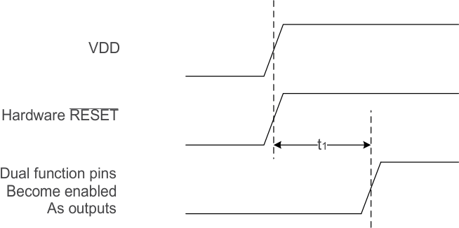 Figure 9-1 Power Up Timing
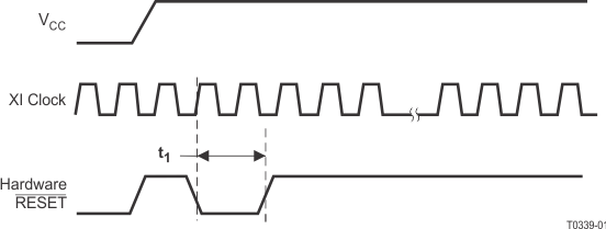 Figure 9-2 Reset Timing
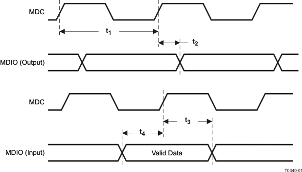 Figure 9-3 MII Serial Management Timing
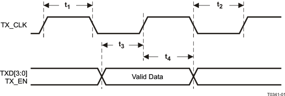 Figure 9-4 100Mb/s MII Transmit Timing
 Figure 9-5 100Mb/s MII Receive Timing
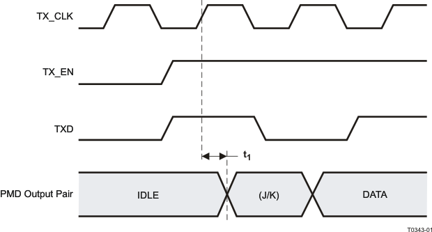 Figure 9-6 100Base-TX Transmit Packet Latency Timing
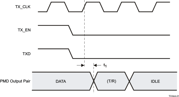 Figure 9-7 100Base-TX Transmit Packet Deassertion Timing
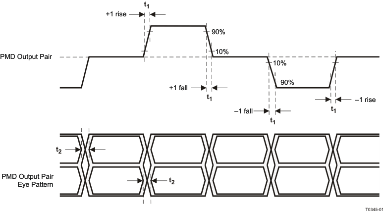 Figure 9-8 100Base-TX Transmit Timing (tR/F and Jitter)
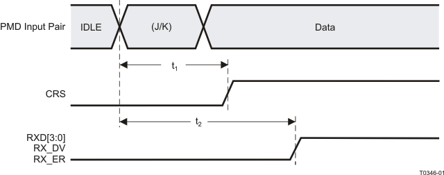 Figure 9-9 100Base-TX Receive Packet Latency Timing
 Figure 9-10 100Base-TX Receive Packet Deassertion Timing
 Figure 9-11 10Mbs MII Transmit Timing
 Figure 9-12 10Mb/s MII Receive Timing
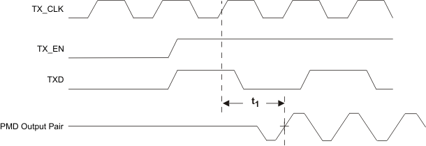 Figure 9-13 10Base-T Transmit Timing (Start of Packet)
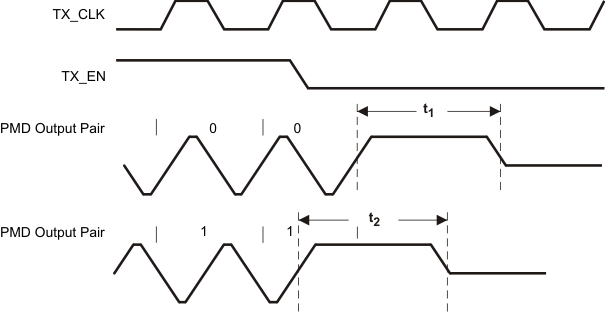 Figure 9-14 10Base-T Transmit Timing (End of Packet)
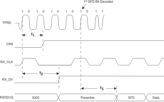 Figure 9-15 10Base-T Receive Timing (Start of Packet)
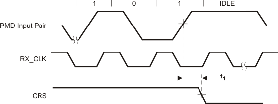 Figure 9-16 10Base-T Receive Timing (End of Packet)
 Figure 9-17 10Mb/s Jabber Timing
 Figure 9-18 10Base-T Normal Link Pulse Timing
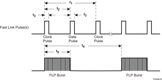 Figure 9-19 Auto-Negotiation Fast Link Pulse (FLP) Timing

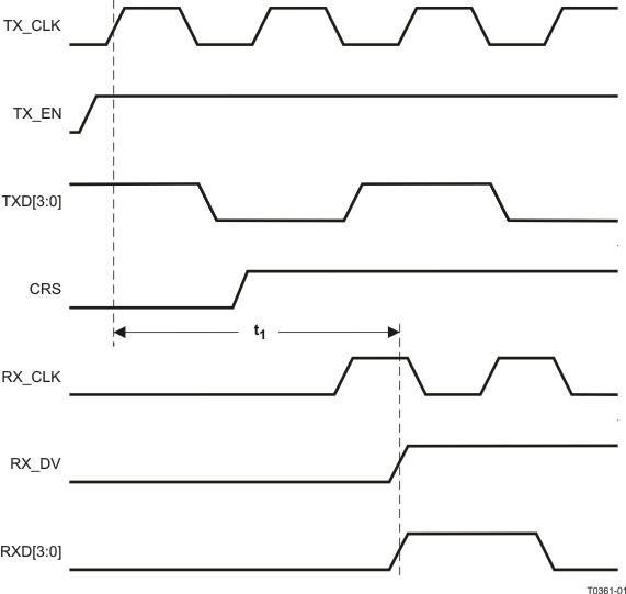
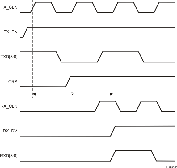
 Figure 9-23 RMII Transmit Timing
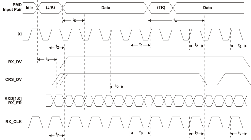 Figure 9-24 RMII Receive Timing
 Figure 9-25 Isolation Timing
 Figure 9-26 25MHz_OUT Timing