JAJSES5Q July 2006 – August 2024 TLK2711-SP
PRODUCTION DATA
- 1
- 1 特長
- 2 アプリケーション
- 3 概要
- 4 Pin Configuration and Functions
-
5 Specifications
- 5.1 Absolute Maximum Ratings
- 5.2 ESD Ratings
- 5.3 Recommended Operating Conditions
- 5.4 Thermal Information
- 5.5 TTL Input Electrical Characteristics
- 5.6 Transmitter/Receiver Electrical Characteristics
- 5.7 Reference Clock (TXCLK) Timing Requirements
- 5.8 TTL Output Switching Characteristics
- 5.9 Typical Characteristics
-
6 Detailed Description
- 6.1 Overview
- 6.2 Functional Block Diagram
- 6.3
Feature Description
- 6.3.1 Transmit Interface
- 6.3.2 Transmit Data Bus
- 6.3.3 Data Transmission Latency
- 6.3.4 8-Bit/10-Bit Encoder
- 6.3.5 Pseudo-Random Bit Stream (PRBS) Generator
- 6.3.6 Parallel to Serial
- 6.3.7 High-Speed Data Output
- 6.3.8 Receive Interface
- 6.3.9 Receive Data Bus
- 6.3.10 Data Reception Latency
- 6.3.11 Serial to Parallel
- 6.3.12 Comma Detect and 8-Bit/10-Bit Decoding
- 6.3.13 LOS Detection
- 6.3.14 PRBS Verification
- 6.3.15 Reference Clock Input
- 6.3.16 Operating Frequency Range
- 6.3.17 Testability
- 6.3.18 Loopback Testing
- 6.3.19 BIST
- 6.3.20 Power-On Reset
- 6.4 Device Functional Modes
- 7 Application and Implementation
- 8 Device and Documentation Support
- 9 Revision History
- 10Mechanical, Packaging, and Orderable Information
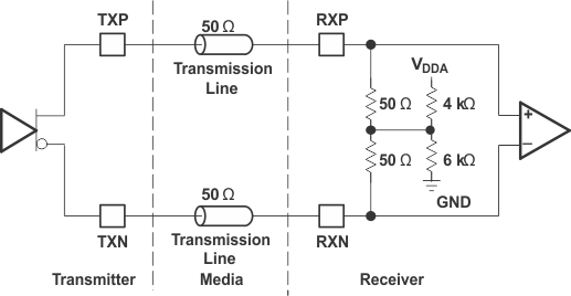
6.4.2 High-Speed I/O Directly-Coupled Mode
 Figure 6-7 High-Speed I/O Directly-Coupled Mode Schematic