JAJSGX9B August   2018  – January 2020 TLV1805-Q1

PRODUCTION DATA.  

  1. 特長
  2. アプリケーション
  3. 概要
    1.     Device Images
      1.      N チャネル MOSFET による逆電流保護
      2.      P チャネル MOSFET による逆電流および過電圧保護
  4. 改訂履歴
  5. Pin Configuration and Functions
    1.     Pin Functions
  6. Specifications
    1. 6.1 Absolute Maximum Ratings
    2. 6.2 ESD Ratings
    3. 6.3 Recommended Operating Conditions
    4. 6.4 Thermal Information
    5. 6.5 Electrical Characteristics
    6. 6.6 Switching Characteristics
    7. 6.7 Typical Characteristics
  7. Detailed Description
    1. 7.1 Overview
    2. 7.2 Functional Block Diagram
    3. 7.3 Feature Description
      1. 7.3.1 Rail to Rail Inputs
      2. 7.3.2 Power On Reset
      3. 7.3.3 High Power Push-Pull Output
      4. 7.3.4 Shutdown Function
      5. 7.3.5 Internal Hysteresis
    4. 7.4 Device Functional Modes
      1. 7.4.1 External Hysteresis
        1. 7.4.1.1 Inverting Comparator With Hysteresis
        2. 7.4.1.2 Noninverting Comparator With Hysteresis
  8. Application and Implementation
    1. 8.1 Application Information
    2. 8.2 Typical Applications
      1. 8.2.1 Design Requirements
      2. 8.2.2 Detailed Design Procedure
      3. 8.2.3 Application Curve
      4. 8.2.4 Reverse Current Protection Using MOSFET and TLV1805-Q1
        1. 8.2.4.1 Minimum Reverse Current
        2. 8.2.4.2 N-Channel Reverse Current Protection Circuit
          1. 8.2.4.2.1 N-Channel Oscillator Circuit
      5. 8.2.5 P-Channel Reverse Current Protection Circuit
      6. 8.2.6 P-Channel Reverse Current Protection With Overvotlage Protection
      7. 8.2.7 ORing MOSFET Controller
  9. Power Supply Recommendations
  10. 10Layout
    1. 10.1 Layout Guidelines
    2. 10.2 Layout Example
  11. 11デバイスおよびドキュメントのサポート
    1. 11.1 ドキュメントのサポート
      1. 11.1.1 関連資料
    2. 11.2 ドキュメントの更新通知を受け取る方法
    3. 11.3 サポート・リソース
    4. 11.4 商標
    5. 11.5 静電気放電に関する注意事項
    6. 11.6 Glossary
  12. 12メカニカル、パッケージ、および注文情報

パッケージ・オプション

メカニカル・データ(パッケージ|ピン)
サーマルパッド・メカニカル・データ
発注情報

Switching Characteristics

Typical values are at TA = 25°C, VS = 12 V, VCM = VS / 2; Input overdrive = 100 mV (unless otherwise noted).
PARAMETER TEST CONDITIONS MIN TYP MAX UNIT
tPHL Propagation delay time, high-to-low (1) CL = 15 pF 250 ns
CL = 4 nF 450 ns
tPLH Propagation delay time, low-to-high (1) CL = 15 pF 250 ns
CL = 4 nF 500 ns
tR Rise time 20% to 80%, CL = 15 pF 18 ns
20% to 80%, CL = 4 nF 0.3 µs
tF Fall time 20% to 80%, CL = 15 pF 10 ns
20% to 80%, CL = 4 nF 0.26 µs
tSTART Power-up time (2) 45 µs
High-to-low and low-to-high refers to the transition at the input.
During power on, VS must exceed 3.3 V for tON before the output is in a correct state.
TLV1805-Q1 propdelay.tifFigure 1. Propagation Delay
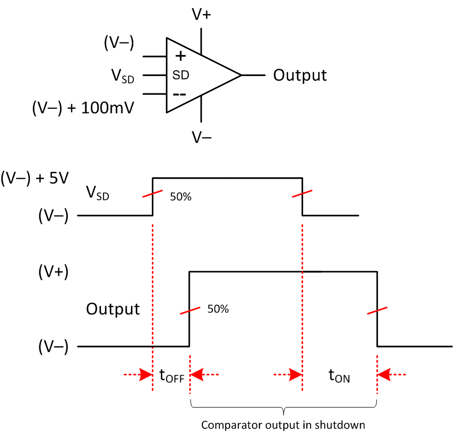
TLV1805-Q1 shutdown.tifFigure 2. Shutdown Timing