JAJSVS4A May   2024  – November 2024 TLV1831 , TLV1832 , TLV1841 , TLV1842

PRODMIX  

  1.   1
  2. 特長
  3. アプリケーション
  4. 概要
  5. Pin Configuration and Functions
    1.     Pin Configuration: TLV1831 and TLV1841
    2.     Pin Configurations: TLV1832 and TLV1842
    3.     Pin Configuration and Functions: TLV1834 and TLV1844
  6. Specifications
    1. 5.1 Absolute Maximum Ratings
    2. 5.2 ESD Ratings
    3. 5.3 Thermal Information
    4. 5.4 Recommended Operating Conditions
    5. 5.5 Electrical Characteristics
    6. 5.6 Switching Characteristics
    7. 5.7 Typical Characteristics
  7. Detailed Description
    1. 6.1 Overview
    2. 6.2 Functional Block Diagrams
    3. 6.3 Feature Description
    4. 6.4 Device Functional Modes
      1. 6.4.1 Inputs
        1. 6.4.1.1 Rail-to-Rail Input
        2. 6.4.1.2 Unused Inputs
      2. 6.4.2 Outputs
        1. 6.4.2.1 TLV183x Push-Pull Output
        2. 6.4.2.2 TLV184x Open-Drain Output
      3. 6.4.3 ESD Protection
        1. 6.4.3.1 Inputs
        2. 6.4.3.2 Outputs
      4. 6.4.4 Power-On Reset (POR)
  8. Application and Implementation
    1. 7.1 Application Information
      1. 7.1.1 Basic Comparator Definitions
        1. 7.1.1.1 Operation
        2. 7.1.1.2 Propagation Delay
        3. 7.1.1.3 Overdrive Voltage
      2. 7.1.2 Hysteresis
        1. 7.1.2.1 Inverting Comparator With Hysteresis
        2. 7.1.2.2 Non-Inverting Comparator With Hysteresis
        3. 7.1.2.3 Inverting and Non-Inverting Hysteresis using Open-Drain Output
    2. 7.2 Typical Applications
      1. 7.2.1 Window Comparator
        1. 7.2.1.1 Design Requirements
        2. 7.2.1.2 Detailed Design Procedure
        3. 7.2.1.3 Application Curve
      2. 7.2.2 Square Wave Oscillator
        1. 7.2.2.1 Design Requirements
        2. 7.2.2.2 Detailed Design Procedure
        3. 7.2.2.3 Application Performance Plots
    3. 7.3 Power Supply Recommendations
    4. 7.4 Layout
      1. 7.4.1 Layout Guidelines
      2. 7.4.2 Layout Example
  9. Device and Documentation Support
    1. 8.1 Documentation Support
      1. 8.1.1 Related Documentation
    2. 8.2 ドキュメントの更新通知を受け取る方法
    3. 8.3 サポート・リソース
    4. 8.4 Trademarks
    5. 8.5 静電気放電に関する注意事項
    6. 8.6 用語集
  10. Revision History
  11. 10Mechanical, Packaging, and Orderable Information

パッケージ・オプション

メカニカル・データ(パッケージ|ピン)
サーマルパッド・メカニカル・データ

Detailed Design Procedure

The oscillation frequency is determined by the resistor and capacitor values. The following calculation provides details of the steps.
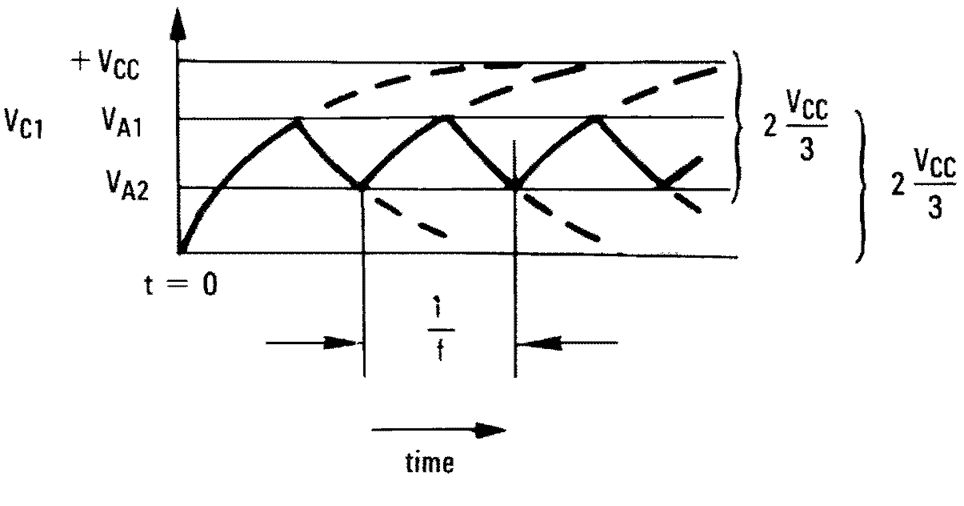
TLV1831 TLV1841 TLV1832 TLV1842  Square-Wave Oscillator Timing ThresholdsFigure 7-10 Square-Wave Oscillator Timing Thresholds

First consider the output of Figure Square-Wave Oscillator as high, which indicates the inverted input VC is lower than the noninverting input (VA). This causes the C1 to be charged through R4, and the voltage VC increases until it is equal to the noninverting input. The value of VA at the point is calculated below.

Equation 7. TLV1831 TLV1841 TLV1832 TLV1842

if R1 = R2= R3, then VA1 = 2VCC/3

At this time the comparator output trips pulling down the output to the negative rail. The value of VAat this point is calculated below.

Equation 8. TLV1831 TLV1841 TLV1832 TLV1842

if R1 = R2 = R3, then VA2 = VCC/3

The C1 now discharges though the R4, and the voltage VCC decreases until it reaches VA2. At this point, the output switches back to the starting state. The oscillation period equals to the time duration from for C1 from 2VCC/3 to VCC / 3 then back to 2VCC/3, which is given by R4C1 × ln 2 for each trip. Therefore, the total time duration is calculated as 2 R4C1 × ln 2.

The oscillation frequency can be obtained below.

Equation 9. TLV1831 TLV1841 TLV1832 TLV1842